Driver circuit

a technology of driving circuit and drive chip, which is applied in the direction of oscillator generator, pulse technique, electronic switching, etc., can solve the problems of affecting the speed of the state change of unable to drive the controlled power semiconductor component, and known gate driver not enabling to control the on-state gate voltage, etc., to achieve limiting temperature variations, limiting radiated interference, and maximising efficiency

Active Publication Date: 2018-09-25
ABB (SCHWEIZ) AG
View PDF6 Cites 0 Cited by
  • Summary
  • Abstract
  • Description
  • Claims
  • Application Information

AI Technical Summary

Benefits of technology

[0011]The invention is based on the idea of arranging multiple of resistors and switches in the driver circuit for providing different control voltages to the output stage of the gate driver. The resistors together with the switches are connected to the auxiliary voltages of the gate driver such that the switches are controlled to provide a selected control voltage for operating the output switches of the output stage of the driver circuit. The resistances of the resistors are selected is such a manner that a variety of control voltages together with selected current levels are available from the driver circuit. As the resistors and the switches are providing voltages and currents to the output switches of the driver circuit, the resistors and the switches can be of small size and power rating. The currents through the components are in the range of milliamperes and therefore the power losses in the driver circuit are minimal.
[0012]The gate driver of the invention is simple and consists of low-cost components and yet the gate driver is able to control the controlled power semiconductor component in separate periods and in effective way. The gate driver of the invention enables to control the switch component such that separate periods of the state change of the switch component are taken into account. With the invention, the current fed to the gate of the controlled semiconductor component and the voltage applied to the gate of the component in different periods can be set. This enables to control the speed of the state change and losses during the state change and during the conduction time. The speed of the switching of the controlled component affects the radiated and conducted interferences and by controlling the losses of the component, the adverse effects of temperature changes can be reduced. Further, the invention can be employed to increase the performance of a device in which the circuit and method are employed, as the switching speed and the gate voltage can be set to highest possible values in each operation point.
[0013]As the gate driver enables a precise control of the controlled component, the parallel use of semiconductor components is simpler without the need of carefully selecting the paralleled components before the use.
[0015]According to embodiments of the invention, the gate voltages and currents can be selected during the use of the component based on multiple of factors, such as limiting the temperature variations, limiting the radiated interferences and maximising efficiency.

Problems solved by technology

The gate resistance limits the current from the output switches of the driver circuit and thereby affects the speed of the state change of the controlled power semiconductor component.
One of the problems associated with the known gate drivers is that they are not able to drive the controlled power semiconductor component, such as an IGBT, in an efficient and controlled manner in which the different periods of turn-on and turn-off processes can be taken into account.
Further, the known gate drivers do not enable to control the on-state gate voltage or to select different turn-on or turn-off speeds during the operation of the device, as these speeds are governed by the gate resistors.
Although this arrangement increases the versatility of control of the switching periods, the arrangement is complicated and requires fast components.

Method used


Image

  • Driver circuit
  • Driver circuit
  • Driver circuit

Examples


Embodiment Construction

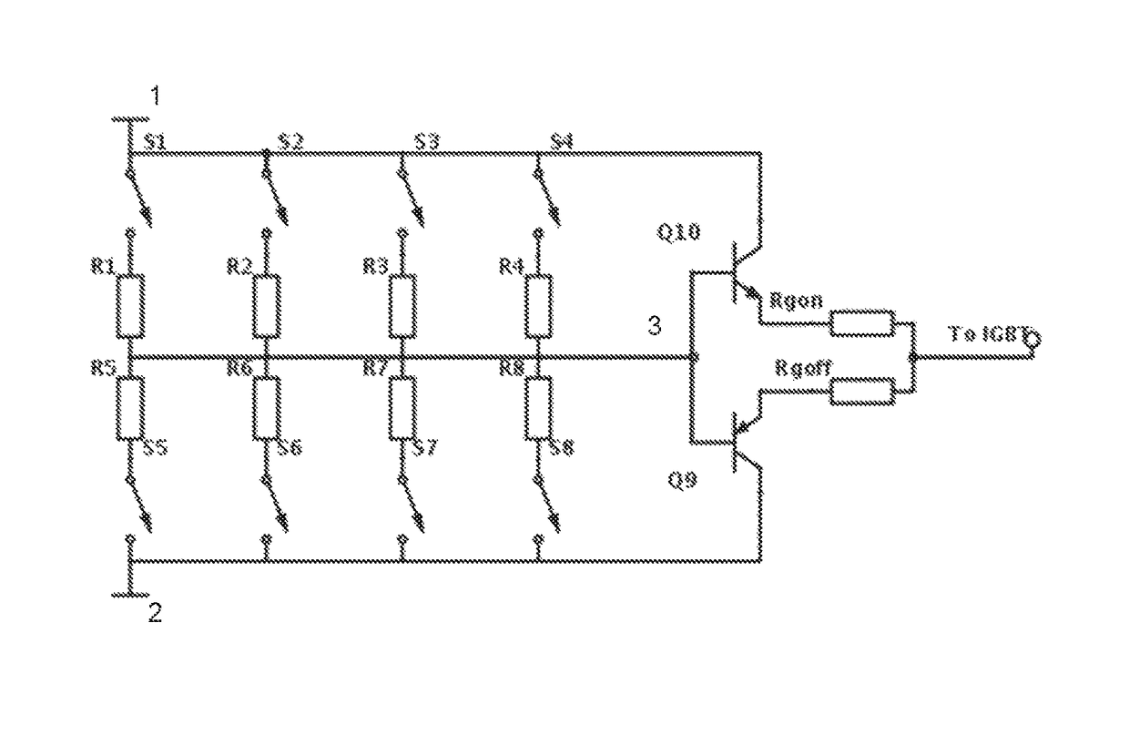
[0024]FIG. 1 shows an embodiment of the gate driver circuit of the invention. The gate driver of the embodiment comprises an output stage composed of output switch components Q9, Q10. The output switches are connected in a known manner between a high auxiliary voltage rail and a low auxiliary voltage rail. The auxiliary voltages are supplied to the rails for providing a voltage difference between the rails. The voltage of the low auxiliary rail may be a negative voltage or a positive voltage. In the following the high auxiliary voltage rail and the low auxiliary voltage rail are referred to as positive auxiliary rail and negative auxiliary rail.

[0025]In the embodiment shown in FIG. 1, the output stage comprises output switches, which are transistors forming a push-pull circuit. In such a circuit, the control electrodes 3 i.e. the bases of the transistors are electrically connected to each other to form the control input of the output stage. In the embodiment of FIG. 1, the output of...


PUM


Abstract

A gate driver circuit and a method of operating a gate driver circuit. The gate driver circuit comprising a high auxiliary voltage rail and a low auxiliary voltage rail for receiving high auxiliary voltage and low auxiliary voltage, output stage connected to the auxiliary voltage rails and comprising a control input and an output terminal for providing an output voltage of the gate driver, plurality of series connections of controllable switches and resistive components, wherein a first part of the plurality of series connections is connected between the high auxiliary voltage rail and control input of the output stage, and a second part of the plurality of series connections is connected between the low auxiliary voltage rail and control input of the output stage, and a control circuit for controlling the controllable switches for providing a control voltage and a control current to the control input of the output stage.

Description

FIELD OF THE INVENTION[0001]The present invention relates to driver circuits, and particularly to a driver circuit for a power semiconductor component.BACKGROUND OF THE INVENTION[0002]Power semiconductor components, such as IGBTs, are used for switching high currents and high voltages in variety of devices. Such devices include power converters that are used for converting electrical power from one form to another. Power converters comprise one or more power semiconductor components that are employed as switches.[0003]When a power semiconductor component is used as a switch, the component operates between a fully conducting state and a blocking state. In the conducting state the switch component provides a low impedance current path and in the blocking state the switch component blocks the current and holds the voltage over the component.[0004]A driver circuit is employed for controlling a power semiconductor component in a desired manner. For an IGBT component, a driver circuit pro...

Claims


Application Information

Patent Timeline
Patent Type & Authority Patents(United States)
IPC IPC(8): H03B1/00H03K17/04H03K17/14H03K17/06
CPCH03K17/0406H03K17/14H03K17/06H03K17/163H03K17/168
Inventor SALMIA, TEEMUKITTILA, JUKKA-PEKKAHERRALA, TEROTAULANNE, MIKKO
Owner ABB (SCHWEIZ) AG
Why Eureka
Try Eureka