Dual ramp pixel readout

a pixel readout and ramp technology, applied in the field of image sensors, can solve the problems of adding complexity to the comparator, saving total conversion time, etc., and achieve the effect of relaxing the adc read nois

Active Publication Date: 2021-11-09
SHENZHEN GOODIX TECH CO LTD
View PDF9 Cites 0 Cited by
  • Summary
  • Abstract
  • Description
  • Claims
  • Application Information

AI Technical Summary

Benefits of technology

[0008]According to yet another aspect, the inventive concept relates to images sensors that perform the reset conversions in parallel as well by adding a second comparator per ADC, so that the conversion can be captured with both ramp rates at the same time during both the reset conversion phase and the signal conversion phase. This embodiment trades off additional area and power consumption for the ADC at the benefit of slightly improved total pixel conversion time. In one embodiment, to save power and silicon area, the second comparator capturing the fast ramp, which is also associated with measuring larger signal from the pixel, may be scaled to smaller area and power compared to the other comparator. This will increase noise, but the shot noise of the signal from the pixel will still be larger in most cases.
[0016]By providing two consecutive ramps during both the reset conversion phase and the signal conversion phase (signal measurement phase), where the first ramp is slow and has a limited swing while the second ramp is fast and covers the full range of pixel outputs, significant relaxation of the ADC read noise without any significant impact to the total noise of the measurement can be achieved.

Problems solved by technology

Since the pixel output requires some time to settle, and the signal has to settle to a level much more precise than what is required for this coarse decision, this is possible to do without adding time to the total conversion time, but adds complexity to the comparator to perform this operation and select one of two ramp inputs.
In theory, this may save total conversion time however.
In either implementation, it is still necessary to perform two reset conversions and they must be performed in series since it is not possible to know ahead of time which conversions will be needed to construct the final ADC output.

Method used


Image

  • Dual ramp pixel readout
  • Dual ramp pixel readout
  • Dual ramp pixel readout

Examples


Embodiment Construction

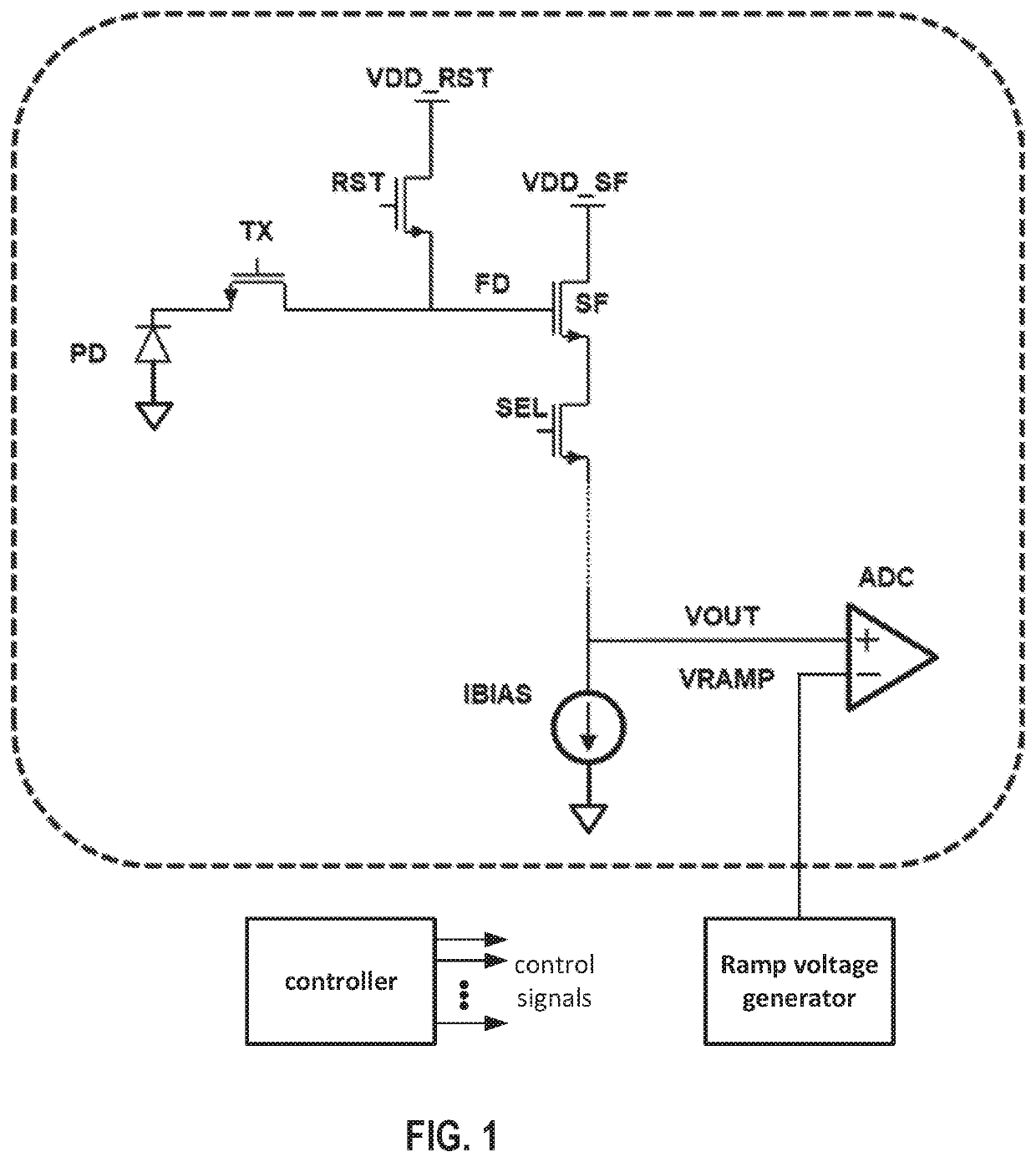
[0028]FIG. 1 is a block diagram of a pixel coupled to an example readout circuit according to an embodiment of the present disclosure. Referring to FIG. 1, the pixel includes a photodiode (or a photosensitive element) PD, a transfer transistor TX coupled to the photodiode PD, a source follower SF having a gate coupled to the transfer transistor TX, a reset transistor RST coupled to a floating diffusion node FD disposed between the transfer transistor TX and the gate of the source follower SF. The reset transistor RST is configured to charge the floating diffusion node FD to the reset voltage VDD_RST when the reset transistor RST is turned on, thereby resetting the floating diffusion node FD. The photodiode PD may be reset along with the floating diffusion node FD by turning on the transfer transistor TX. The source follower SF has a terminal coupled to the source follower voltage VDD_SF and another terminal coupled to a select transistor SEL. The select transistor SEL has a gate cou...


PUM


Abstract

An image sensor includes a plurality of pixel columns and a plurality of readout circuits. Each readout circuit is coupled to one of the plurality of pixel columns and includes an ADC for receiving a first analog signal of a pixel in a reset conversion phase and a second analog signal of the pixel in a signal measurement phase, a dual-ramp generator for generating a first ramp having a first ramp rate and a second ramp having a second ramp rate greater than the first ramp rate and providing the first ramp to the readout circuits in the reset conversion phase and the second ramp to the plurality of readout circuits in the signal measurement phase, and a controller configured to provide control signals to the readout circuits and the dual-ramp generator.

Description

TECHNICAL FIELD OF THE INVENTION[0001]The present invention relates to CMOS image sensors, and more particularly, to an image sensor and method for operating thereof using a dual-ramp generator.BACKGROUND OF THE INVENTION[0002]Modern image sensors with high pixel count attempt to achieve high frame rate, low read noise and high dynamic range with minimal power consumption. The basic function of a modern CMOS image sensor (CIS) is to capture photons that are converted into electrons in a photo diode. These captured electrons are read out by a series of analog-to-digital converters (ADCs) included as part of the image sensor. In particular, it is very challenging in a single image frame to readout pixels that have received a large number of electrons at the same time as achieving low noise readout for pixels that have received a small number of electrons. This is defined as the dynamic range of the image sensor, which is the maximum electrons that can be read out divided by the number...

Claims


Application Information

Patent Timeline
Patent Type & Authority Patents(United States)
IPC IPC(8): H04N5/363H04N5/374
CPCH04N5/363H04N5/3742H03M1/123H03M1/56H04N25/75H04N25/65H04N25/767
Inventor POWELL, MATTHEWELSAYED, MOHAMED
Owner SHENZHEN GOODIX TECH CO LTD
Why Eureka
Try Eureka