Electrostatic discharge protection semiconductor device and layout structure of ESD protection semiconductor device
a technology of esd protection and semiconductor devices, applied in semiconductor devices, diodes, electrical devices, etc., can solve the problems of increasing the vulnerability of external environment, increasing the risk of esd to modern electronics, and increasing the difficulty so as to improve the machine model of esd protection semiconductor devices
- Summary
- Abstract
- Description
- Claims
- Application Information
AI Technical Summary
Benefits of technology
Problems solved by technology
Method used
Image

Examples
Embodiment Construction
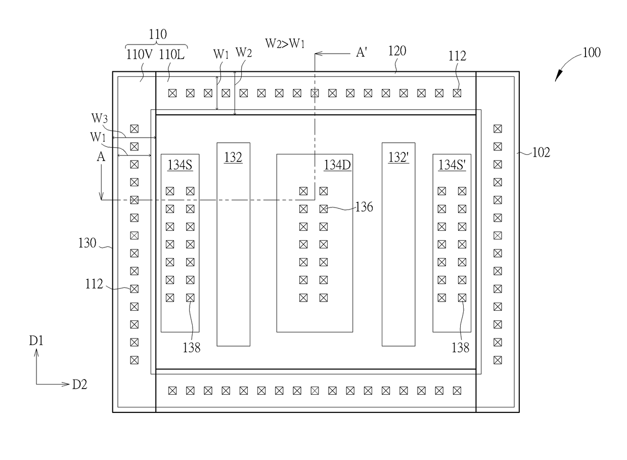
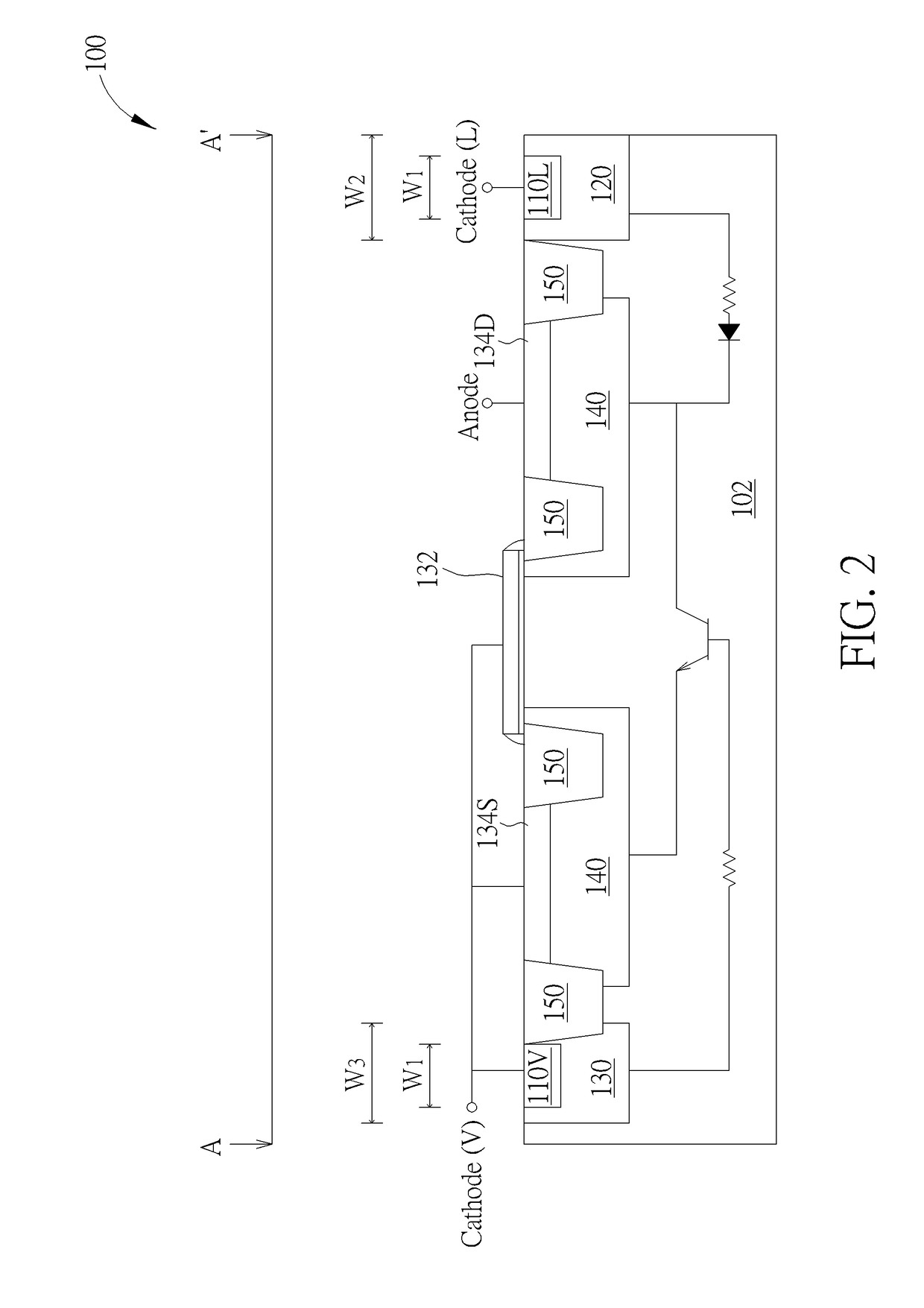
[0015]Please refer to FIGS. 1 and 2, wherein FIG. 1 is a schematic drawing illustrating a layout structure of an ESD protection semiconductor device provided by a first preferred embodiment of the present invention, and FIG. 2 is a schematic drawing illustrating the ESD protection semiconductor device provided by the first preferred embodiment. Particularly, FIG. 2 is a cross-sectional view taken along a line A-A′ of FIG. 1. As shown in FIGS. 1 and 2, the preferred embodiment provides a layout structure of an ESD protection semiconductor device 100 and an ESD protection semiconductor device 100. The ESD protection semiconductor device 100 and its layout structure 100 include a substrate 102. The substrate 102 includes a first conductivity type. In some embodiments of the present invention, the substrate 102 can be a well region formed in a wafer, but not limited to this. According to the preferred embodiment, the first conductivity type is a p type. In other words, the substrate 102...
PUM
 Abstract
Description
Claims
Application Information