
Semiconductor structures and fabrication methods thereof

a technology of semiconductor devices and structures, applied in the direction of semiconductor devices, electrical equipment, transistors, etc., can solve the problems of affecting the performance of semiconductor devices, affecting the uniform width, and severe leakage current problems

Active Publication Date: 2018-10-09
SEMICON MFG INT (SHANGHAI) CORP +1
View PDF13 Cites 2 Cited by
  • Summary
  • Abstract
  • Description
  • Claims
  • Application Information

AI Technical Summary

Benefits of technology

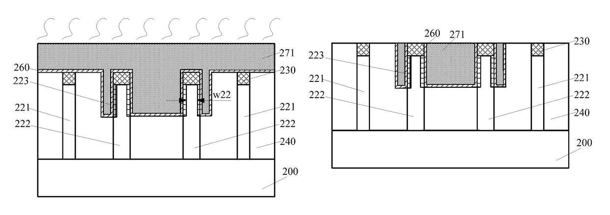
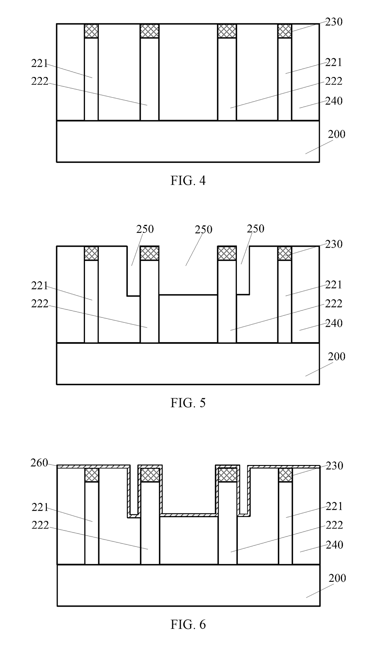
[0105]For example, according to the disclosed fabrication methods, by performing an oxygen annealing process during a fluid CVD process to form the second isolation film, the second fin structure may be treated by the oxygen annealing process. Specifically, during the oxygen annealing process, the surface portion of the sidewalls of each second fin structure may be oxidized so that the width of the portion of the second fin structure exposed in the trenches may be reduced due to water vapor treatment. Therefore, the difference between the width of the portion of the second fin structure exposed in the trenches and the width of each first fin structure, i.e. the first width, may be smaller than the difference between the initial width of each second fin structure and the width of each first fin structure. Therefore, the uniformity of the width of the first fin structures, i.e. the first width, and the second fin structures, i.e. the second width, may be improved. Moreover, no additional oxygen treatment process may be required, and thus the fabrication process may be simplified.

Problems solved by technology

With continuous development of semiconductor technology, traditional planar MOS transistor exhibits weak controllability on the channel current, causing severe leakage current issues.
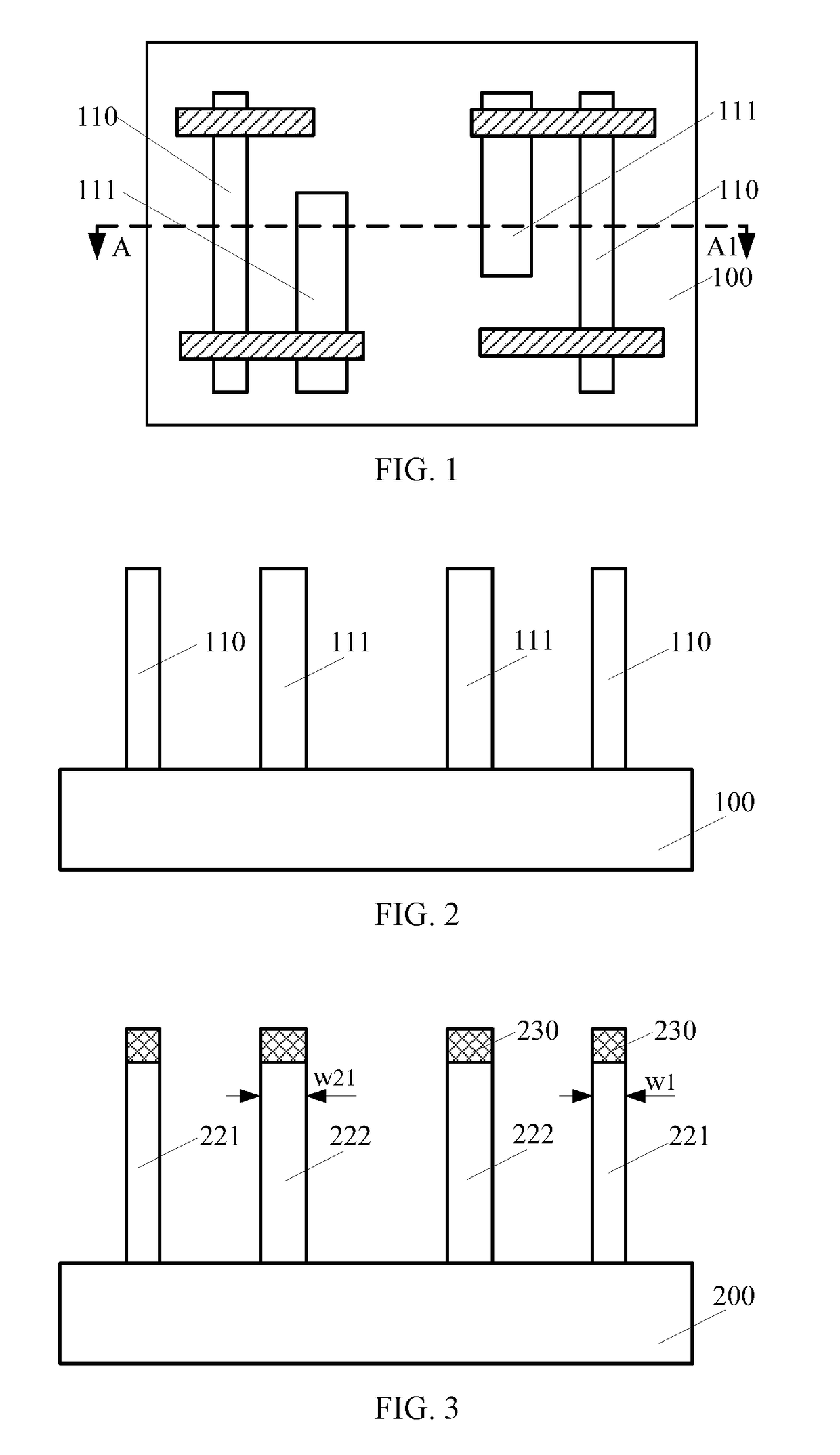
However, for semiconductor devices formed by existing Fin-FETs, the fin structures may still not have a uniform width and the lack of fin width consistency may further affect the performance of the semiconductor devices.

Method used


Image

  • Semiconductor structures and fabrication methods thereof
  • Semiconductor structures and fabrication methods thereof
  • Semiconductor structures and fabrication methods thereof

Examples


Embodiment Construction

[0014]Reference will now be made in detail to exemplary embodiments of the invention, which are illustrated in the accompanying drawings. Wherever possible, the same reference numbers will be used throughout the drawings to refer to the same or like parts.

[0015]For semiconductor devices fabricated by existing methods, the fin structures may not have a uniform fin width.

[0016]FIG. 1 shows a schematic cross-section view of a semiconductor structure. FIG. 2 shows a schematic cross-section view of the semiconductor structure shown in FIG. 1 along an A-A1 line.

[0017]Referring to FIG. 1, the semiconductor device is a static random-access memory (SRAM) device. The semiconductor device includes a semiconductor substrate 100, two first fin structures 110 formed on the semiconductor substrate 100, and a fin structure group including two adjacent second fin structures 111 formed on the semiconductor substrate. The two first fin structures are situated on the two opposite sides of the fin struc...


PUM


Abstract

Semiconductor structure and fabrication method thereof are provided. An exemplary method includes providing a semiconductor substrate including a plurality of first fin structures, each having a first width, and a plurality of second fin structures, each having a second width greater than the first width. The method further includes forming a first isolation film covering sidewall surfaces of the first fin structures and the second fin structures, forming a trench in the first isolation film to expose at least a top portion of at least one sidewall surface of one or more second fin structures, forming an isolation fluid layer to fill the trenches, and performing an oxygen annealing process to convert a surface layer of the top portion of the at least one sidewall surface of the one or more second fin structures into a by-product layer, and to convert the isolation fluid layer into a second isolation film.

Description

CROSS-REFERENCES TO RELATED APPLICATIONS[0001]This application claims the priority of Chinese Patent Application No. CN201610646944.5, filed on Aug. 9, 2016, the entire content of which is incorporated herein by reference.FIELD OF THE DISCLOSURE[0002]The present disclosure generally relates to the field of semiconductor fabrication technology and, more particularly, relates to semiconductor structures and fabrication methods thereof.BACKGROUND[0003]Metal-oxide-semiconductor (MOS) transistor is one of the most important components in modern integrated circuits (ICs). A basic structure of a MOS transistor includes a semiconductor substrate, a gate structure formed on the surface of the semiconductor substrate, and doped source / drain regions formed in the semiconductor substrate on the two sides of the gate structure. Usually, the gate structure includes a gate dielectric layer formed on the surface of the semiconductor substrate and a gate electrode layer formed on the surface of the ...

Claims


Application Information

Patent Timeline
Patent Type & Authority Patents(United States)
IPC IPC(8): H01L21/76H01L29/66H01L29/10H01L29/06H01L21/762H01L21/8234H01L27/088H01L21/02H01L27/11
CPCH01L21/823412H01L21/02236H01L21/76224H01L21/823431H01L27/0886H01L29/0653H01L29/1037H01L29/66818H01L21/823481H01L27/1104H01L29/1033H01L29/66795H10B10/12
Inventor ZHOU, FEI
Owner SEMICON MFG INT (SHANGHAI) CORP
Learn More