Dual constant time switching regulator and switching control circuit and method thereof

a constant time switching and control circuit technology, applied in the direction of power conversion systems, dc-dc conversion, instruments, etc., can solve the problems of large voltage drop on the output voltage vo, large ripple in the output voltage, and unstable output performan

Active Publication Date: 2018-10-09
RICHTEK TECH
View PDF1 Cites 0 Cited by
  • Summary
  • Abstract
  • Description
  • Claims
  • Application Information

AI Technical Summary

Benefits of technology

[0014]From another perspective, the present invention provides a method for controlling a dual constant time switching regulator, wherein the dual constant time switching regulator comprises a power circuit which includes an inductor and at least a power switch and is configured to operably convert an input voltage to an output voltage; the method including: comparing a first input signal and a second input signal to generate a comparison result, wherein the first input signal and the second input signal are one of the following combinations: (1) the first input signal is a triangle wave signal, and the second input signal is an error amplified signal; or (2) the first input signal is the output voltage related signal, and the second input signal is a reference voltage; and generating a switch control signal according to the comparison result to control the power switch, wherein the power switch keeps ON for at least a minimum ON time after the power switch is turned ON, and after the minimum ON time finishes, the power switch keeps ON until the level of the first input signal is higher than the level of the second input signal, and at this time point the power switch is turned OFF, wherein the power switch keeps OFF for at least a minimum OFF time after the power switch is turned OFF, and after the minimum OFF time finishes, the power switch keeps OFF until the level of the first input signal is lower than the level of the second input signal, and at this time point the power switch is turned ON.
[0015]In one embodiment, the step of generating the triangle wave includes: generating the triangle wave signal according to the switch control signal and / or an output current related signal.

Problems solved by technology

A drawback of the prior art shown in FIG. 1A is that: since the ON time is constant and a minimum OFF time is required, the maximum rising slope of the inductor current ILD is limited by the constant ON time TON and the minimum OFF time, and therefore during fast load transient, a large voltage drop will occur on the output voltage VO.
Besides, because the ON time is constant and the minimum OFF time is required, the duty cycle is limited and cannot be adjusted to a higher ratio (for example close to 100%); therefore, when the input voltage VIN is close to the output voltage VO during buck power conversion, the power switches S1 and S2 have to switch by a high switching frequency, causing large ripple in the output voltage and unstable output performance.
However, in an integrated PMIC (Power Management Integrated Circuit) which controls multiple switching regulators, one VOS pin is required for each switching regulator, which increases the cost and the complexity of the PCB layout.

Method used


Image

  • Dual constant time switching regulator and switching control circuit and method thereof
  • Dual constant time switching regulator and switching control circuit and method thereof
  • Dual constant time switching regulator and switching control circuit and method thereof

Examples


Embodiment Construction

[0025]The drawings as referred to throughout the description of the present invention are for illustration only, to show the interrelations between the circuits and the signal waveforms, but not drawn according to actual scale.

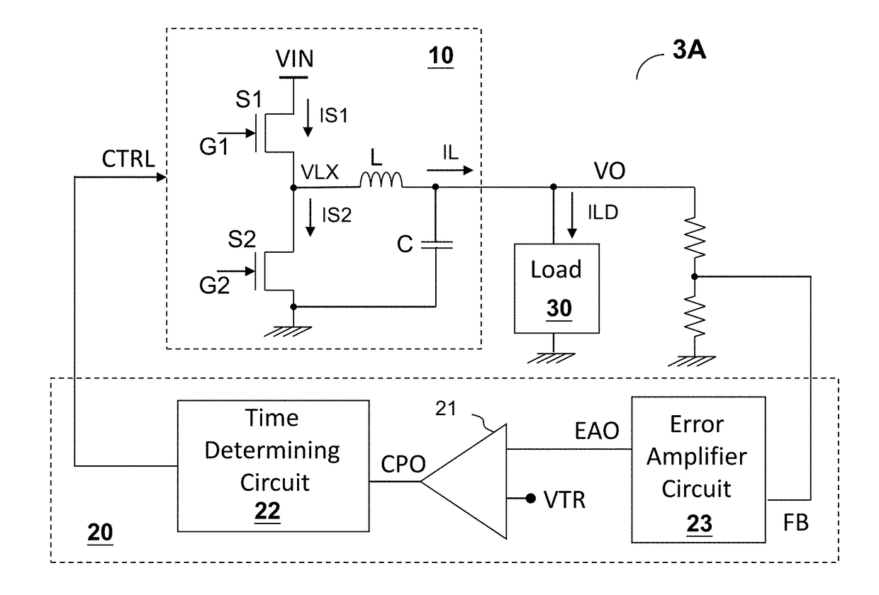
[0026]FIG. 3A shows an embodiment of a dual constant time switching regulator (switching regulator 3A) according to the present invention. The switching regulator 3A comprises a buck power circuit 10 and a switching control circuit 20. The buck power circuit 10 includes an inductor L and power switches S1 and S2, and is configured to operably convert the input voltage VIN to and output voltage VO.

[0027]The control circuit 20 generates a switch control signal CTRL (which for example includes G1 and G2) according to an output voltage related signal to control the power switches S1 and S2, wherein the output voltage related signal may be for example a feedback signal FB as shown in the figure or the output voltage itself. The switching control circuit 20 includes...


PUM


Abstract

A dual constant time switching regulator includes: a power circuit including an inductor and at least a power switch for converting an input power to an output power, and a switching control circuit for generating a switch control signal to control the power switch, wherein the switching control circuit includes a comparison circuit for comparing an error amplified signal and a triangle wave signal to generate a comparison result, and a time determining circuit for generating the switch control signal according to the comparison result, wherein after the power switch turns ON, it keeps ON for at least a minimum ON time until the triangle wave signal is higher than the error amplified signal, and wherein after the power switch turns OFF, it keeps OFF for at least a minimum OFF time and until the triangle wave signal is lower than the error amplified signal.

Description

CROSS REFERENCE[0001]The present invention claims priority to CN201710638973.1, filed on Jul. 31, 2017.BACKGROUND OF THE INVENTIONField of Invention[0002]The present invention relates to a constant time switching regulator; particularly, it relates to a switching regulator with two sets of constant time. The present invention also relates to a switching control circuit and a control method of a switching regulator.Description of Related Art[0003]FIG. 1A shows a prior art constant time switching regulator (switching regulator 1A). The switching regulator 1A comprises a buck power circuit 10 which includes an inductor L and power switches S1 and S2, and a control circuit 50. The control circuit 50 controls the power switches S1 and S2 to convert an input voltage VIN to an output voltage VO. In the control circuit 50, an error amplifier 51 compares a feedback signal FB (which relates to the output voltage VO) with a reference voltage VR to generate an error amplified signal EAO. APWM (...

Claims


Application Information

Patent Timeline
Patent Type & Authority Patents(United States)
IPC IPC(8): G05F1/00H02M1/088H02M1/14H02M3/158H02M1/00
CPCH02M1/14H02M1/088H02M3/158H02M2001/0029H02M3/156H02M1/0029H02M3/1566
Inventor CHENG, HUNG-YUWU, KUO-CHUN
Owner RICHTEK TECH
Why Eureka
Try Eureka