Method for manufacturing an electrical contact on a structure

a manufacturing method and technology for electrical contacts, applied in the direction of electric discharge lamps, basic electric elements, electric apparatus, etc., can solve the problems of difficult to make a true edge contact, difficult to implement, and difficult to connect these structures to the outside world using electrodes

Active Publication Date: 2018-11-20
COMMISSARIAT A LENERGIE ATOMIQUE ET AUX ENERGIES ALTERNATIVES
View PDF10 Cites 0 Cited by
  • Summary
  • Abstract
  • Description
  • Claims
  • Application Information

AI Technical Summary

Benefits of technology

[0025]Moreover the presence of the electrode during the implantation step protects the structure. In effect, by way of an example, the Applicant has observed that carbon nanotubes are destroyed, at least locally (at the implanted volume) if they are implanted before formation of the electrode.
[0026]Furthermore, the method according to the invention requires less severe cleaning conditions before formation of the electrode. In effect, the implantation step encourages closer contact between the electrode and the structure. This effect is particularly advantageous in the case of a structure made of carbon nanotubes or of graphene, in which contamination with carbon-containing products is very difficult to reduce. The method according to the invention is consequently less sensitive to contamination.
[0031]The formation of the chemical bonds between the species M and the anisotropic material allows effective introduction of electrons into the structure, in the manner of edge contacts described earlier.

Problems solved by technology

Connecting these structures to the outside world using electrodes can present certain difficulties, however.
True edge contact is, however, difficult to implement.
Consequently top contacts are by far the most widely used, on the one hand since they are technically simpler to make than an edge contact, and on the other hand since it is very difficult to make a true edge contact.
Therefore an interface material may not be available or may require operating conditions which are incompatible with the nature of the structure 1 (for example the material may require high temperatures for its formation).
The formation of cavities however requires the use of a photo-lithographic step which because of its resolution does not allow electrodes of small size, for example of less than 50 nm, to be formed.
Furthermore, this technique cannot easily be implemented on a structure 1 made of carbon nanotubes.
This method however cannot be performed on transition dichalcogenide molecules (for example MoS2).
This method therefore only applies to carbon nanomaterials and may be difficult to implement in the case of two-dimensional compounds, for example.

Method used


Image

  • Method for manufacturing an electrical contact on a structure
  • Method for manufacturing an electrical contact on a structure
  • Method for manufacturing an electrical contact on a structure

Examples


Embodiment Construction

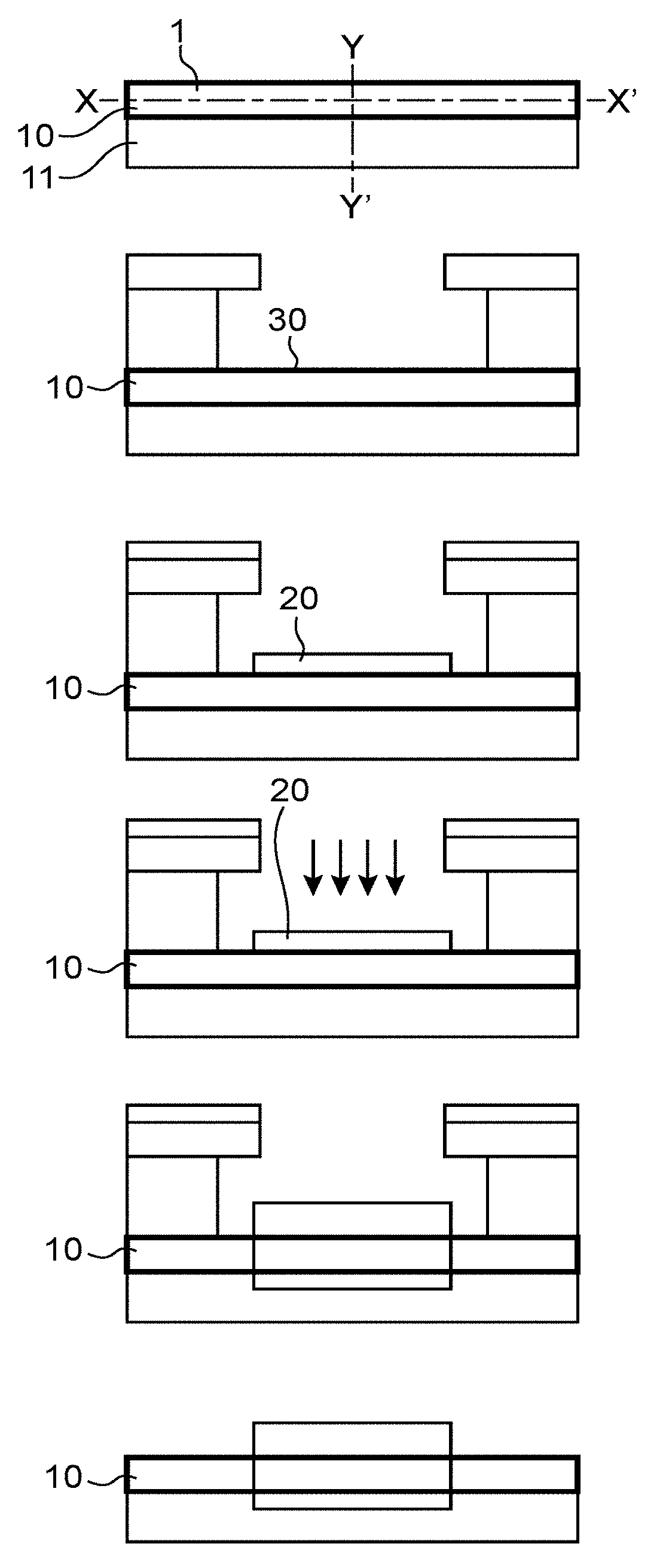
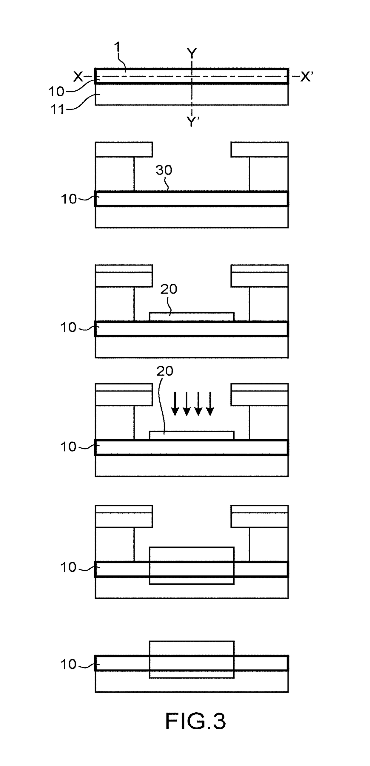
[0020]The aims of the invention are achieved, at least in part, by a method for manufacture of an electrical contact on a structure made of anisotropic material NA which exhibits an anisotropic electrical conductivity, where the structure exhibits an axial electrical conductivity σ / / along a first axis XX′ of the structure and at least one orthogonal electrical conductivity σ⊥ along at least one direction YY′ orthogonal to the first axis XX′ of the structure, where the at least one electrical conductivities σ⊥ are less than the axial electrical conductivity σ / / , where the method comprises:[0021]a step for the formation of an electrode with an initial thickness Ei comprising at least one species M, on a first surface of the structure, where the first surface is orthogonal to the at least one directions YY′;[0022]the electrode formation step is followed by a step of implantation of species X through the electrode, into the structure.

[0023]Thus the implantation step can be used to de-s...


PUM


Abstract

The invention relates to a method for manufacture of an electrical contact on a structure (10) made of an anisotropic material NA which exhibits an anisotropic electrical conductivity, where the structure (10) exhibits an axial electrical conductivity along a first axis XX′ of the structure (10) and an orthogonal conductivity along a direction YY′ orthogonal to the first axis XX′ of the structure (10), where the orthogonal conductivity is less than the axial conductivity, where the method comprises:a step for the formation of a conductive electrode (20), with an initial thickness Ei, comprising a species M, on a first surface (30) of the structure (10), where the first surface (30) is orthogonal to the orthogonal direction YY′;the method being characterized in that the step for the formation of the conductive electrode (20) is followed by a step for implantation of species X through the conductive electrode (20), into the structure (10).

Description

TECHNICAL FIELD[0001]The invention relates to a method for manufacturing an electrical contact on a structure. More specifically the invention relates to a method for making an electrical contact on a structure made of a material which exhibits anisotropic electrical conductivity.STATE OF THE PRIOR ART[0002]Structures made of materials which exhibit anisotropic electrical properties such as carbon nanotubes are very promising for applications in the fields of microelectronics, spintronics, opto-electronics, sensors or transparent electrical conductors.[0003]Connecting these structures to the outside world using electrodes can present certain difficulties, however. Indeed, even though the creation of electrodes which exhibit a low contact resistivity on materials such as silicon is well understood by those skilled in the art, the opposite is not true when the structure is made of an anisotropic material and exhibits anisotropy in terms of electrical conductivity (hereafter referred t...

Claims


Application Information

Patent Timeline
Patent Type & Authority Patents(United States)
IPC IPC(8): H01L21/265H01L21/02
CPCH01L21/265H01J2893/0022H01L21/02527H01L21/02606H01L21/02601H01L21/02603H01L21/02568H10K71/30H10K85/221
Inventor RAMOS, RAPHAELDIJON, JEAN
Owner COMMISSARIAT A LENERGIE ATOMIQUE ET AUX ENERGIES ALTERNATIVES
Why Eureka
Try Eureka