Semiconductor device

a technology of semiconductor chips and semiconductor wiring layers, which is applied in the direction of semiconductor/solid-state device details, instruments, optical elements, etc., can solve the problems etc., and achieve the effect of difficult to reduce the size of semiconductor chips and restricted layout of electric wiring layers

Active Publication Date: 2017-12-05
RENESAS ELECTRONICS CORP
View PDF4 Cites 4 Cited by
  • Summary
  • Abstract
  • Description
  • Claims
  • Application Information

AI Technical Summary

Benefits of technology

[0004]No electric wiring layer is formed right above an optical waveguide made of silicon (Si) in general. This is for the purpose of preventing the light (referred to also as Evanescent light or near-field light) which has leaked out when optical signals propagate through an optical waveguide from being reflected by the electric wiring layer located right above it and interfering with the optical signals propagating through the optical waveguide. For this reason, however, the layout of the electric wiring layer is restricted, and this makes it difficult to reduce the size of the semiconductor chip.
[0007]According to the embodiment, it is possible to achieve the size reduction of the semiconductor chip.

Problems solved by technology

For this reason, however, the layout of the electric wiring layer is restricted, and this makes it difficult to reduce the size of the semiconductor chip.

Method used


Image

  • Semiconductor device
  • Semiconductor device
  • Semiconductor device

Examples


first embodiment

[0027](First Embodiment)

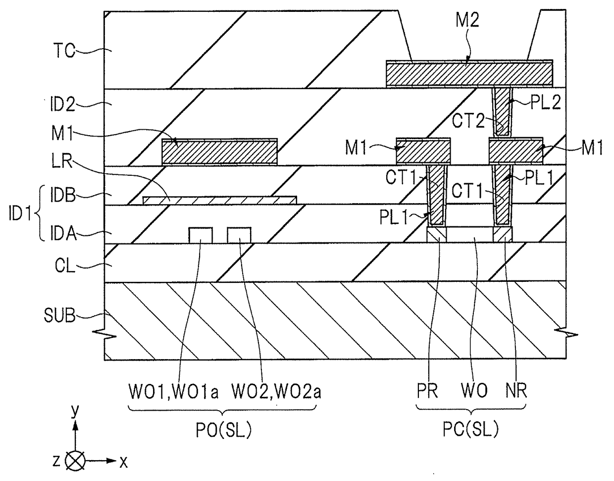
[0028]In recent years, the development of the technology to realize an optical communication module by fabricating an optical signal transmission line made of silicon (Si) and integrating various optical devices and electronic devices with using an optical circuit constituted of the optical signal transmission line as a platform, that is, the silicon photonics technology has been actively pursued.

[0029]The technology disclosed in the first embodiment is applied in particular to an optical device among various devices constituting a semiconductor device using the silicon photonics technology. For this reason, in the following description, a structure and a manufacturing method of an optical device integrated on an SOI (Silicon On Insulator) substrate will be described. In addition, in the following description, an optical directional coupler and an optical modulator are illustrated as examples of optical devices and a multilayer wiring with a two-layer structu...

second embodiment

[0076](Second Embodiment)

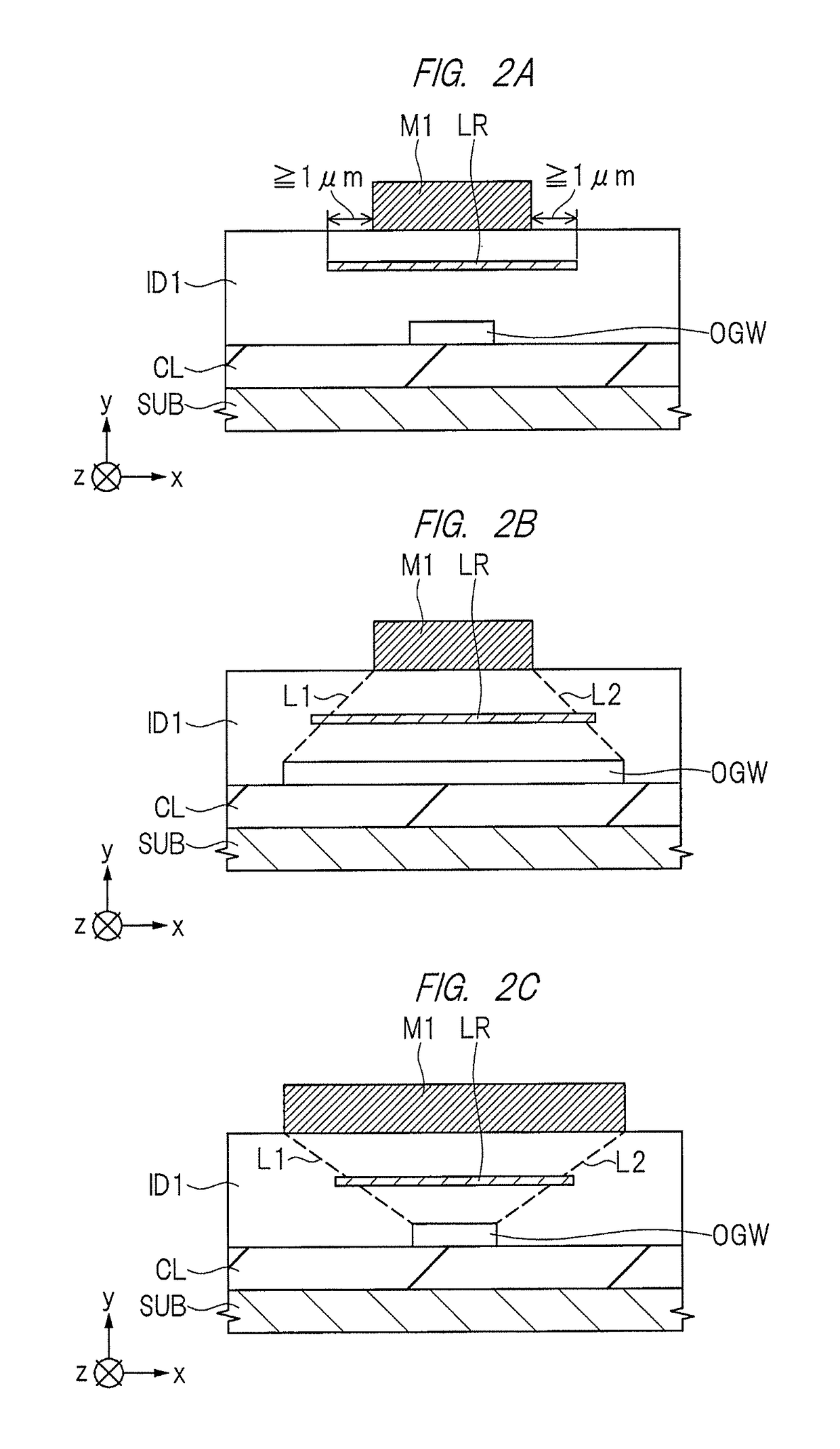
[0077]The second embodiment differs from the first embodiment described above in the arrangement of the low reflectance film LR. Namely, in the first embodiment described above, the first interlayer insulating film ID1 which covers the first-layer wiring M1 is constituted of the lower-layer insulating film IDA and the upper-layer insulating film IDB, and the low reflectance film LR is formed between the lower-layer insulating film IDA and the upper-layer insulating film IDB. In the second embodiment, however, the low reflectance film LR is formed between the first interlayer insulating film ID1 and the first-layer wiring M1 so as to be in contact with the first-layer wiring M1.

[0078]Since the semiconductor device of the second embodiment is almost the same as the semiconductor device of the first embodiment described above except for the arrangement of the low reflectance film LR, the difference will be mainly described below.

[0079]

[0080]The structure of the...

third embodiment

[0087](Third Embodiment)

[0088]The third embodiment differs from the first embodiment described above in the arrangement of the low reflectance film LR. Namely, in the first embodiment described above, the first interlayer insulating film ID1 which covers the first-layer wiring M1 is constituted of the lower-layer insulating film IDA and the upper-layer insulating film IDB, and the low reflectance film LR is formed between the lower-layer insulating film IDA and the upper-layer insulating film IDE. In the third embodiment, however, the low reflectance film LR is formed on a lower surface and a side surface of the first-layer wiring M1 so as to be in contact with the first-layer wiring M1.

[0089]Since the semiconductor device of the third embodiment is almost the same as the semiconductor device of the first embodiment described above except for the arrangement of the low reflectance film LR, the difference will be mainly described below.

[0090]

[0091]The structure of the semiconductor d...


PUM

PropertyMeasurementUnit
reflectanceaaaaaaaaaa
thicknessaaaaaaaaaa
thicknessaaaaaaaaaa

Abstract

A low reflectance film with a second reflectance (50% or lower) lower than a first reflectance is formed between an optical directional coupler and a first-layer wiring with the first reflectance. Thus, even when the first-layer wiring is formed above the optical directional coupler, the influence of the light reflected by the first-layer wiring on the optical signal propagating through the first optical waveguide and the second optical waveguide of the optical directional coupler can be reduced. Accordingly, the first-layer wiring can be arranged above the optical directional coupler, and the restriction on the layout of the first-layer wiring is relaxed.

Description

CROSS-REFERENCE TO RELATED APPLICATION[0001]The present application claims priority from Japanese Patent Application No. 2015-099864 filed on May 15, 2015, the content of which is hereby incorporated by reference into this application.TECHNICAL FIELD OF THE INVENTION[0002]The present invention relates to a semiconductor device, and can be effectively applied to, for example, a semiconductor device having various optical devices in a semiconductor chip.BACKGROUND OF THE INVENTION[0003]Japanese Patent Application Laid-Open Publication No. 2012-027198 (Patent Document 1) describes an optical semiconductor device including an optical waveguide formed of a part of a semiconductor layer, a first impurity region which is formed in the semiconductor layer on one side of the optical waveguide and to which an impurity of a first conductivity type is introduced and a second impurity region which is formed in the semiconductor layer on the other side of the optical waveguide and to which an imp...

Claims


Application Information

Patent Timeline
Patent Type & Authority Patents(United States)
IPC IPC(8): G02B6/26G02B6/132G02F1/025H01L23/532G02B6/125G02B6/12G02B6/28
CPCG02F1/025G02B6/125G02B6/132H01L23/53214H01L23/53228G02F2201/08G02B6/2852G02B2006/12061G02B2006/12142G02B2006/12147H01L2224/05
Inventor KUNISHIMA, HIROYUKINAKASHIBA, YASUTAKAWAKABAYASHI, MASARUWATANUKI, SHINICHI
Owner RENESAS ELECTRONICS CORP
Why Eureka
Try Eureka