
Semiconductor device
a technology of semiconductor chips and semiconductor wiring layers, which is applied in the direction of semiconductor/solid-state device details, instruments, optical elements, etc., can solve the problems etc., and achieve the effect of difficult to reduce the size of semiconductor chips and restricted layout of electric wiring layers
- Summary
- Abstract
- Description
- Claims
- Application Information
AI Technical Summary
Benefits of technology
Problems solved by technology
Method used
Image

Examples
first embodiment
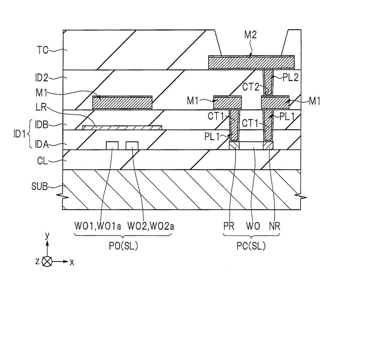
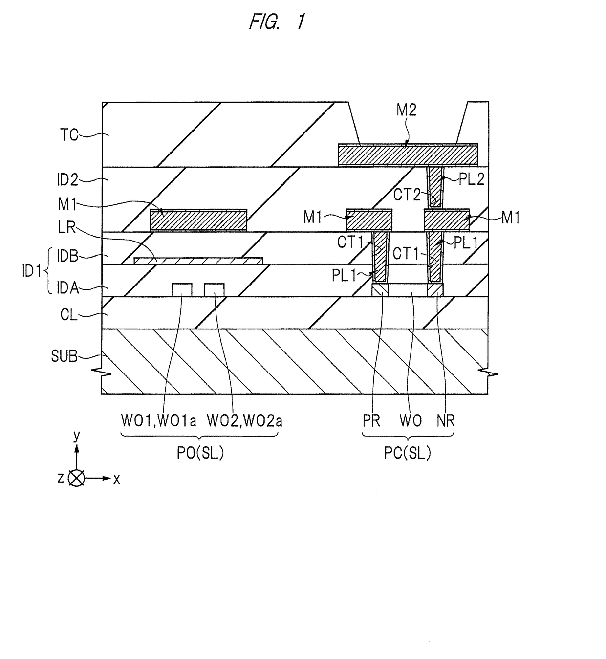
[0027]In recent years, the development of the technology to realize an optical communication module by fabricating an optical signal transmission line made of silicon (Si) and integrating various optical devices and electronic devices with using an optical circuit constituted of the optical signal transmission line as a platform, that is, the silicon photonics technology has been actively pursued.
[0028]The technology disclosed in the first embodiment is applied in particular to an optical device among various devices constituting a semiconductor device using the silicon photonics technology. For this reason, in the following description, a structure and a manufacturing method of an optical device integrated on an SOI (Silicon On Insulator) substrate will be described. In addition, in the following description, an optical directional coupler and an optical modulator are illustrated as examples of optical devices and a multilayer wiring with a two-layer structure is illustrated as an ...
second embodiment
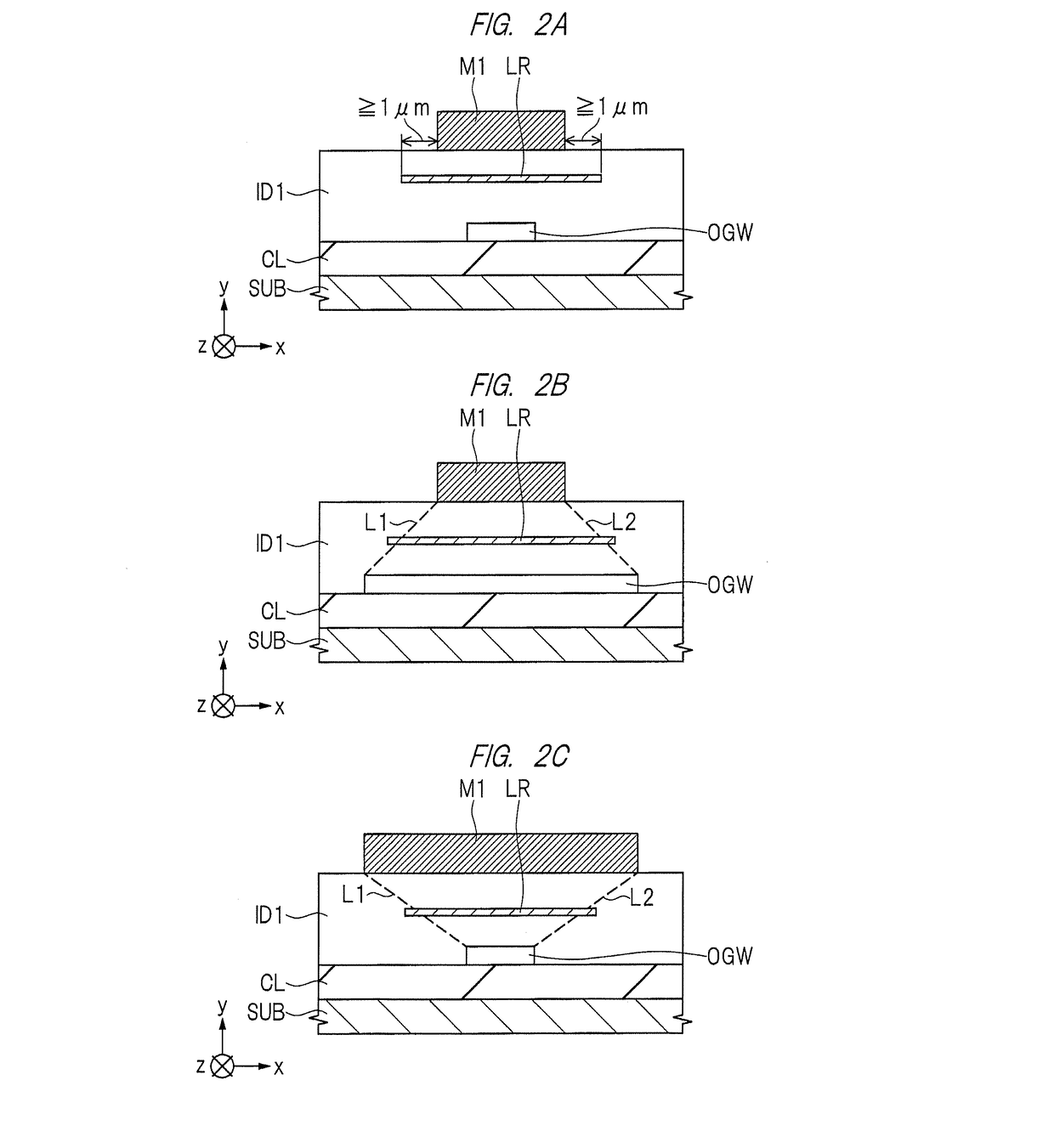
[0075]The second embodiment differs from the first embodiment described above in the arrangement of the low reflectance film LR. Namely, in the first embodiment described above, the first interlayer insulating film ID1 which covers the first-layer wiring M1 is constituted of the lower-layer insulating film IDA and the upper-layer insulating film IDB, and the low reflectance film LR is formed between the lower-layer insulating film IDA and the upper-layer insulating film IDB. In the second embodiment, however, the low reflectance film LR is formed between the first interlayer insulating film ID1 and the first-layer wiring M1 so as to be in contact with the first-layer wiring M1.
[0076]Since the semiconductor device of the second embodiment is almost the same as the semiconductor device of the first embodiment described above except for the arrangement of the low reflectance film LR, the difference will be mainly described below.
[0077]
[0078]The structure of the semiconductor device acc...
third embodiment
[0085]The third embodiment differs from the first embodiment described above in the arrangement of the low reflectance film LR. Namely, in the first embodiment described above, the first interlayer insulating film ID1 which covers the first-layer wiring M1 is constituted of the lower-layer insulating film IDA and the upper-layer insulating film IDB, and the low reflectance film LR is formed between the lower-layer insulating film IDA and the upper-layer insulating film IDB. In the third embodiment, however, the low reflectance film LR is formed on a lower surface and a side surface of the first-layer wiring M1 so as to be in contact with the first-layer wiring M1.
[0086]Since the semiconductor device of the third embodiment is almost the same as the semiconductor device of the first embodiment described above except for the arrangement of the low reflectance film LR, the difference will be mainly described below.
[0087]
[0088]The structure of the semiconductor device according to the t...
PUM
| Property | Measurement | Unit |
|---|---|---|
| reflectance | aaaaa | aaaaa |
| reflectance | aaaaa | aaaaa |
Abstract
Description
Claims
Application Information