
Semiconductor device

a technology of semiconductor devices and semiconductors, applied in semiconductor devices, semiconductor/solid-state device details, electrical apparatus, etc., can solve the problems of deteriorating the electric insulation between the first signal terminal and the second signal terminal, and the adhesion probably deteriorates the electric insulation

Active Publication Date: 2018-12-18
TOYOTA JIDOSHA KK
View PDF9 Cites 0 Cited by
  • Summary
  • Abstract
  • Description
  • Claims
  • Application Information

AI Technical Summary

Benefits of technology

The present invention provides a semiconductor device that prevents or reduces deterioration of electric insulation between signal terminals caused by grease. The semiconductor device is designed to be placed between cooling units and has a special surface configuration that guides the flow of grease away from the signal terminals, maintaining electrical insulation. This design prevents the grease from flowing to the signal terminals and ensures reliable performance under vibration and temperature cycling.

Problems solved by technology

However, the grease having flowed to the top surface of the sealing body expands to the minimum creepage path between the first signal terminals and the second signal terminals, and if electrically-conductive foreign substances, such as metallic powders, adhere to the grease, this adhesion probably deteriorates the electric insulation between the first signal terminals and the second signal terminals.

Method used


Image

  • Semiconductor device
  • Semiconductor device
  • Semiconductor device

Examples


Embodiment Construction

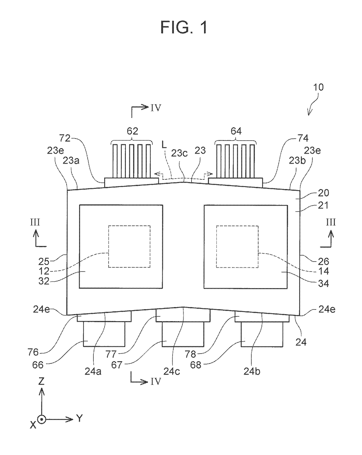
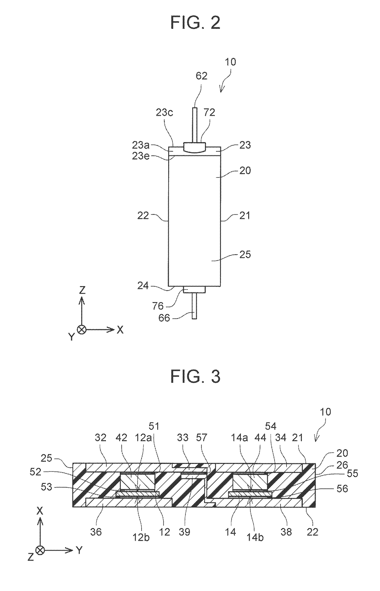
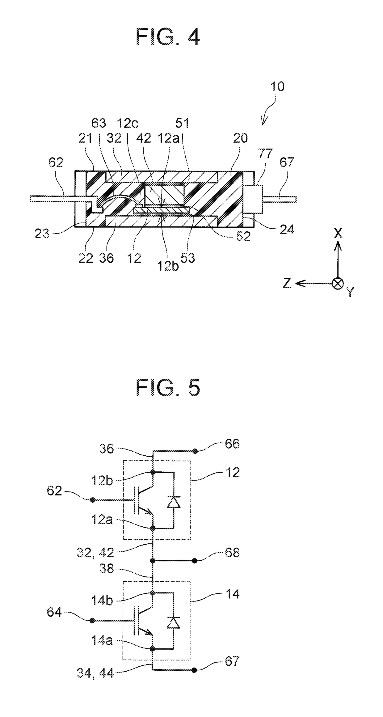
[0028]With reference to drawings, a semiconductor device 10 of an embodiment will be described. As an example, the semiconductor device 10 of the present embodiment is used for an electric power converting apparatus 100 (see FIG. 6 and others) for converting and controlling electric power, and configures upper and lower arms of a kind of an inverter circuit. As shown in FIG. 1 to FIG. 5, the semiconductor device 10 includes a first semiconductor element 12, a second semiconductor element 14, and a sealing body 20 that seals the first semiconductor element 12 and the second semiconductor element 14. Each of the first semiconductor element 12 and the second semiconductor element 14 has an allowable current of 100 A or more, and belongs to a power semiconductor element. As shown in FIG. 5, the first semiconductor element 12 and the second semiconductor element 14 are electrically connected in series to each other. As an example, each of the first semiconductor element 12 and the second...


PUM


Abstract

A semiconductor device includes: a sealing body that seals a first semiconductor element and a second semiconductor element; first heat-radiating members exposed at a front surface of the sealing body; second heat-radiating members exposed at a back surface of the sealing body; first signal terminals electrically connected to the first semiconductor element, and projecting from a top surface of the sealing body in a first direction; and second signal terminals electrically connected to the second semiconductor elements, and projecting from the top surface of the sealing body in the first direction. The top surface of the sealing body includes a first inclined surface, a second inclined surface, and a boundary line or a boundary range located therebetween. The boundary line or the boundary range includes at least part of a minimum creepage path between the first signal terminals and the second signal terminals.

Description

CROSS-REFERENCE TO RELATED APPLICATIONS[0001]This application claims priority to Japanese Patent Application No. 2015-237927 filed on Dec. 4, 2015, which is incorporated herein by reference in its entirety including the specification, drawings and abstract.BACKGROUND[0002]1. Technical Field[0003]A disclosure in the present specification relates to a semiconductor device.[0004]2. Description of Related Art[0005]A semiconductor device is disclosed in Japanese Patent Application Publication No. 2015-095560. This semiconductor device includes a first semiconductor element, a second semiconductor element, a sealing body that seals the first semiconductor element and the second semiconductor element, first heat-radiating members exposed at a front surface of the sealing body, second heat-radiating members exposed at a back surface of the sealing body, and plural first signal terminals and plural second signal terminals that project from the top surface of the sealing body. Each of the fir...

Claims


Application Information

Patent Timeline
Patent Type & Authority Patents(United States)
IPC IPC(8): H01L23/31H01L23/367H01L25/11H01L23/00
CPCH01L23/3675H01L23/3121H01L2924/13091H01L2924/13055H01L2224/73265H01L2224/73215H01L2224/48247H01L2224/48091H01L2224/33181H01L2224/32245H01L24/32H01L24/33H01L24/48H01L24/73H01L25/117H01L2224/04042H01L2224/291H01L2924/00014H01L2924/00012H01L2924/014
Inventor HATASA, KEITAIMAI, MAKOTOOKUMURA, TOMOMI
Owner TOYOTA JIDOSHA KK
Learn More