
Charged particle beam device, electron microscope and sample observation method

a charge particle and beam technology, applied in the direction of basic electric elements, electric discharge tubes, electrical equipment, etc., can solve the problems of inability to capture the original structure of biological tissue, protein contained in the sample may be destroyed, etc., and achieve the effect of stable observation and high accuracy

Active Publication Date: 2019-02-12
HITACHI HIGH-TECH CORP
View PDF11 Cites 0 Cited by
  • Summary
  • Abstract
  • Description
  • Claims
  • Application Information

AI Technical Summary

Benefits of technology

[0017]According to one aspect of the present invention, it can be determined whether or not a sample after a pre-process is appropriate for observation with an electron microscope, and it is possible to perform high accuracy and stable observation of the electron microscope.
[0018]In addition, according to one aspect of the present invention, it is possible to observe the electron microscope while maintaining a favorable frozen state by adjusting an observation condition according to the state of the sample.
[0019]Problems, configurations, and effects other than those described above will be clarified from the

Problems solved by technology

In the chemical fixing method, since tissue is dyed with heavy metal, it is possible to observe a structure with clear contrast, but protein contained in the sample may be destroyed, and it is impossible to capture the original structure of the biological tissue.

Method used


Image

  • Charged particle beam device, electron microscope and sample observation method
  • Charged particle beam device, electron microscope and sample observation method
  • Charged particle beam device, electron microscope and sample observation method

Examples


example 1

[0045]TEM or STEM described in the literature of the Background art uses high-acceleration voltage with acceleration voltage of 80 kV to 300 kV. On the other hand, recently, an STEM detector has been attached to the SEM with acceleration voltage of 30 kV as maximum acceleration voltage, and it has been also possible to observe a transmission image at 30 kV.

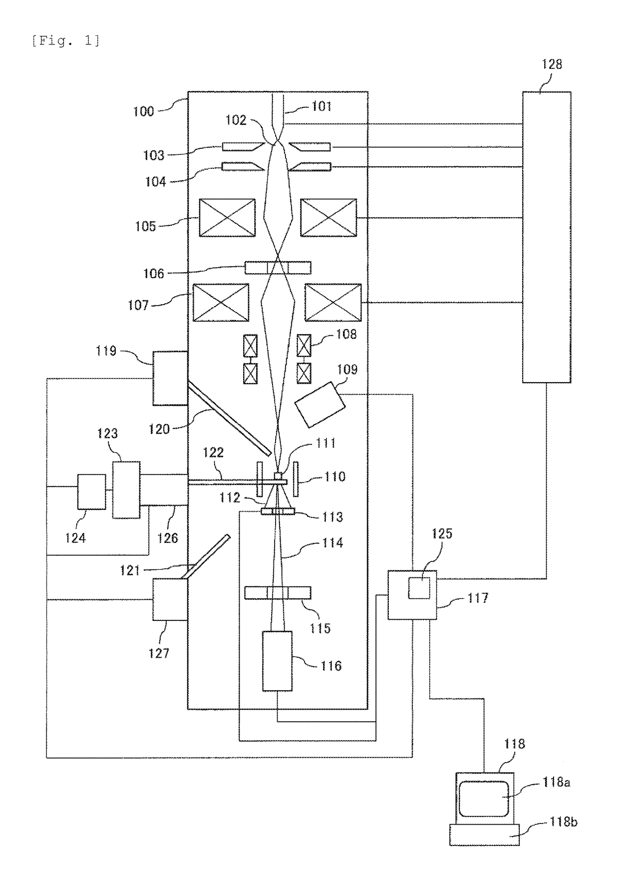
[0046]In the present example, the basic embodiments of the present invention will be described. FIG. 1 is a diagram illustrating a basic configuration of a charged particle beam device according to the present example. In FIG. 1, a configuration of the SEM having the STEM detector and capable of observing an STEM image as an example of the charged particle beam device will be described. However, the present embodiment is not limited thereto, and it can be applied to, for example, the TEM or STEM having the SEM detector and capable of observing the SEM image.

[0047]The SEM illustrated in FIG. 1 is mainly configured to have an SEM le...

example 2

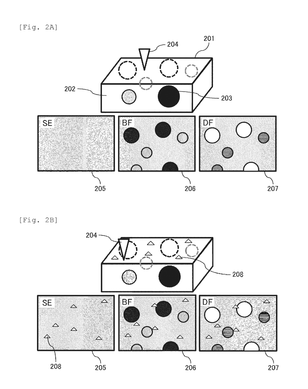
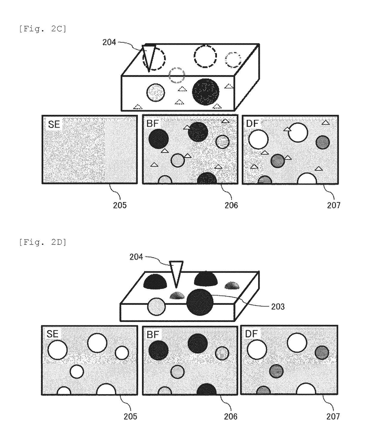
[0059]FIGS. 2A to 2E illustrate observation examples of samples produced by an ice embedding method.

[0060]FIG. 2A is a schematic view of a normal ice embedded sample and a schematic view of an observation result. In a sample 201 produced by the ice embedding method, a structure 203 is contained in an amorphous ice 202 while maintaining an original structure of the structure 203. When an electron beam 204 scans the sample 201, a secondary electron image (hereinafter, referred to as SE) 205 illustrates a surface of the amorphous ice 202 and unevenness information represented as a contrast change cannot be obtained. On the other hand, the structure 203 can be checked by contrast difference in a bright field image (hereinafter, referred to as BF) 206 or a dark field image (hereinafter, referred to as DF) 207 which is a transmitted electron signal.

[0061]FIG. 2B is an observation example in a case where a sample is contained in amorphous ice but a frost 208 is attached to a surface of the...

example 3

[0065]FIG. 3 is a diagram for explaining functions and processes of the image process control unit 125 of FIG. 1. The image process control unit 125 determines whether or not the frozen sample 111 is in an appropriate frozen state and controls a vacuum atmosphere in order to observe stably.

[0066]The frozen sample 111 such as an ice embedded sample is fixed to the sample cooling holder 122 and introduced into the SEM lens tube 100 at a temperature which can maintain a frozen state, for example, from −90° C. to −170° C. After the sample cooling holder 122 is introduced, a temperature and a degree of vacuum of the sample cooling holder 122, and a current position of the tip of the cold trap 120 are measured, and a result thereof is input to the image process control unit 125.

[0067]For example, measured results of the temperature and the degree of vacuum of the cooled sample holder 122 and the position of the cold trap 120 are respectively input to a holder temperature adjustment unit 3...


PUM


Abstract

Provided is an electron microscope with which a sample can be observed stably and with high accuracy. The electron microscope comprises: a sample stage; an electron optical system that scans an electron beam over a sample; a vacuum system that maintains the sample stage and the electron optical system in a vacuum; a secondary electron detector that detects secondary electrons emitted from the sample; transmitted electron detectors that detect transmitted electrons that have transmitted through the sample; and a control device that obtains a secondary electron image and a transmitted electron image on the basis of the secondary electrons and the transmitted electrons detected by the secondary electron detector and the transmitted electron detectors and stores the secondary electron image and the transmitted electron image. The sample stage is provided with cooling means for cooling the sample. The vacuum system is provided with a cold trap that sucks moisture from around the sample and a vacuum gauge that measures the degree of vacuum of the vacuum system.

Description

TECHNICAL FIELD[0001]The present invention relates to a charged particle beam device, an electron microscope, and a sample observation method preferable for maintaining a favorable frozen state of an observation sample.BACKGROUND ART[0002]In recent years, an electron microscope such as a Scanning-Electron-Microscopy (hereinafter, referred to as SEM), a Transmission-Electron-Microscopy (hereinafter, referred to as TEM), a Scanning-Transmission-Electron-Microscopy (hereinafter, also referred to as STEM), or the like has been used for observation and analysis of samples with a fine tissue structure.[0003]Currently, for observation of biological samples using the electron microscope, samples fixed by pre-process are used. For fixation of the sample, there are a chemical fixing method using a reducing agent such as glutaraldehyde as a fixing solution and a physical fixing method of stopping movement instantaneously by rapid freezing and retaining a structure at that time.[0004]In the che...

Claims


Application Information

Patent Timeline
Patent Type & Authority Patents(United States)
IPC IPC(8): H01J37/00H01J37/28H01J37/20H01J37/18
CPCH01J37/28H01J37/18H01J37/20H01J2237/2802H01J2237/2001H01J2237/2004H01J2237/1825
Inventor SUNAOSHI, TAKESHINAGAKUBO, YASUHIRANIMURA, KAZUTAKA
Owner HITACHI HIGH-TECH CORP
Learn More