Electro-optical device, method of manufacturing electro-optical device, and electronic apparatus

a manufacturing method and electrooptical technology, applied in semiconductor devices, capacitors, instruments, etc., can solve problems such as uneven display, defects such as display unevenness, and the inability to realize a capacitance element capable of securing a desired electric capacitance with a smaller occupation area, and achieve good display effect and excellent display quality

Active Publication Date: 2019-04-23
SEIKO EPSON CORP
View PDF16 Cites 0 Cited by
  • Summary
  • Abstract
  • Description
  • Claims
  • Application Information

AI Technical Summary

Benefits of technology

[0008]According to this application example, a second layer stacked on a first layer with an insulating property is in a state of protruding like an eave on an inner side of a trench. Thus, as compared with a case where a capacitance element is simply provided in the trench, a first capacitance electrode, a first capacitance insulating film, and a second capacitance electrode are also provided on a surface of the second layer protruding from the trench, and thereby, it is possible to increase a substantial electric capacitance of the capacitance element. In other words, it is possible to provide an electro-optical device which includes a capacitance element having a larger electric capacitance than before and can realize excellent display quality, even if a pixel size in a planar view is reduced to achieve high definition.
[0026]According to this application, an electro-optical device includes a capacitance element having a desired electric capacitance capable of holding a potential based on an image signal applied to a pixel, and thus, it is possible to provide an electronic apparatus that has excellent display quality and can perform good-looking display.

Problems solved by technology

By doing so, electric capacitance of the capacitance element is reduced, and thereby, a potential written in the pixel is hard to be sufficiently held, and there is a possibility that defects such as display unevenness may be generated.
In other words, there is a problem that realization of a capacitance element capable of securing a desired electric capacitance with a smaller occupation area is required.

Method used


Image

  • Electro-optical device, method of manufacturing electro-optical device, and electronic apparatus
  • Electro-optical device, method of manufacturing electro-optical device, and electronic apparatus
  • Electro-optical device, method of manufacturing electro-optical device, and electronic apparatus

Examples


first embodiment

Electro-Optical Device

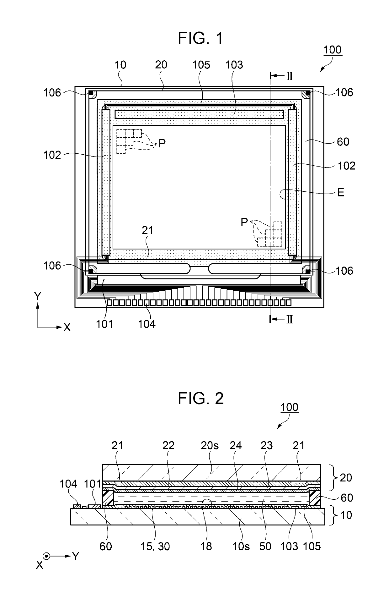
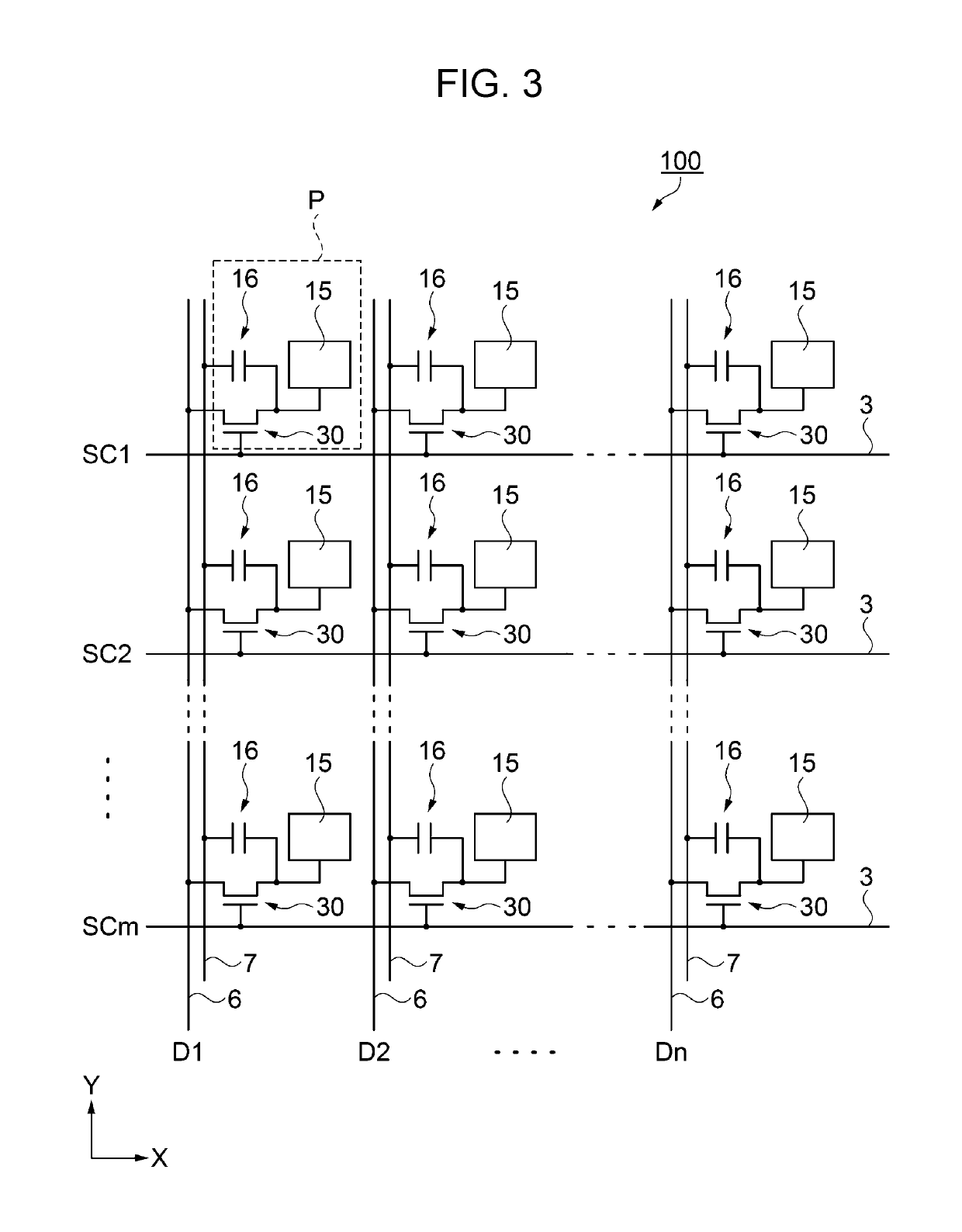
[0052]To begin with, a configuration of a liquid crystal device that is used as an electro-optical device according to the present embodiment will be described with reference to FIG. 1 to FIG. 3. FIG. 1 is a schematic plan view illustrating a configuration of the liquid crystal device. FIG. 2 is a schematic sectional view taken along the line II-II of the liquid crystal device illustrated in FIG. 1, and FIG. 3 is an equivalent circuit diagram illustrating an electrical configuration of the liquid crystal device.

[0053]As illustrated in FIG. 1 and FIG. 2, a liquid crystal device 100 according to the present embodiment includes an element substrate 10 and a counter substrate 20 that are disposed to face each other, and a liquid crystal layer 50 that is interposed between a pair of the substrates. A base member 10s of the element substrate 10 and a base member 20s of the counter substrate 20 use a light-transmittance material, such as a quartz substrate or a glass ...

second embodiment

[0130]Next, a liquid crystal device according to the second embodiment will be described with reference to FIGS. 19 and 20. FIG. 19 is a schematic plan view illustrating arrangement of TFTs and retention capacitors in an element substrate of the liquid crystal device according to the second embodiment, and FIG. 20 is a schematic cross-sectional view illustrating a structure of the element substrate taken along a line XX-XX of FIG. 19.

[0131]A liquid crystal device 200 according to the second embodiment is different from the liquid crystal device 100 according to the first embodiment in configuration of the retention capacitor 16. Thus, the same reference numerals or symbols are attached to the same configuration as those of the liquid crystal device 100 according to the first embodiment, and a detailed description thereof will be omitted.

[0132]As illustrated in FIG. 19, the liquid crystal device 200 according to the present embodiment includes an element substrate 210 having the TFTs...

third embodiment

Electronic Apparatus

[0142]Next, a projection type display device will be described as an example with reference to FIG. 21 as an electronic apparatus to which the liquid crystal device according to each of the above-described embodiments is applied. FIG. 21 is a schematic view illustrating a configuration of the projection type display device as the electronic apparatus.

[0143]As illustrated in FIG. 21, the projection type display device 1000 that is used as an electronic apparatus according to the present embodiment includes a polarized light illumination device 1100 disposed along a system optical axis L and two dichroic mirrors 1104 and 1105 that is used as light separating elements. In addition, three reflection mirrors 1106, 1107, and 1108, and five relay lenses 1201, 1202, 1203, 1204, and 1205 are included in the projection type display device. Furthermore, transmission type liquid crystal light valves 1210, 1220, and 1230 that are used as three optical modulation units, a cros...


PUM

PropertyMeasurementUnit
light transmittanceaaaaaaaaaa
temperatureaaaaaaaaaa
thicknessaaaaaaaaaa

Abstract

A liquid crystal device as an electro-optical device includes a first insulating layer as a first layer with an insulating property stacked on a base member as a substrate, a trench provided in the first insulating layer for each pixel, a second insulating layer as a second layer stacked on the first insulating layer and having an aperture communicating with the trench, and a retention capacitor as a capacitance element including a first capacitance electrode, a first capacitance insulating film, and a second capacitance electrode which are provided on at least an inner side the trench and the aperture. A layer thickness of the first insulating layer is larger than a layer thickness of the second insulating layer, and a width of the trench is larger than a width of the aperture in the X direction as a first direction.

Description

BACKGROUND1. Technical Field[0001]The present invention relates to an electro-optical device, a method of manufacturing an electro-optical device, and an electronic apparatus including the electro-optical device.2. Related Art[0002]An active drive type liquid crystal display device including a transistor which controls switching of a pixel electrode for each pixel is known as an electro-optical device. The liquid crystal display device includes a capacitance element for holding a potential written in a pixel in response to an image signal for each pixel.[0003]For example, JP-A-2000-171827 discloses a liquid crystal display panel in which a trench is provided on an upper surface of a substrate and at least a part of an auxiliary capacitance electrode, an insulating film, and a pixel electrode is provided in the trench, as an electro-optical device including the capacitance element. According to JP-A-2000-171827, an auxiliary capacitor is formed by overlapping the auxiliary capacitanc...

Claims


Application Information

Patent Timeline
Patent Type & Authority Patents(United States)
IPC IPC(8): H01L27/12G02F1/1362H01L29/786G02F1/1368H01L49/02G02F1/1343G02F1/1339G02F1/1335
CPCG02F1/136213G02F1/1368H01L27/1222H01L27/1255H01L27/1259H01L28/91H01L29/78621H01L29/78633H01L29/78675G02F1/1339G02F1/13439G02F1/133512G02F2201/121G02F1/134309G02F1/1309G02F2202/00G02F1/133388G02F1/133562
Inventor SUGIMOTO, YOHEI
Owner SEIKO EPSON CORP
Why Eureka
Try Eureka