Reducing series resistance between source and/or drain regions and a channel region

a technology of series resistance and drain region, applied in the field of semiconductor devices, can solve the problems of poor transistor gate control, inconvenient use, and inability to accurately place dopants and junctions, and achieve the effect of reducing the series resistance of transistors and increasing the lattice structure of materials

Active Publication Date: 2019-06-11
INT BUSINESS MASCH CORP
View PDF13 Cites 0 Cited by
  • Summary
  • Abstract
  • Description
  • Claims
  • Application Information

AI Technical Summary

Benefits of technology

[0003]In accordance with an embodiment, a structure for reducing series resistance for transistors is provided. The structure includes a conductive gate formed over and insulated from a semiconductor substrate, source and / or drain regions formed within the substrate, and source and / or drain extension regions formed within the substrate and adjacent to respective source and / or drain regions. The source and / or drain extension regions are formed from a material alloyed with a first dopant and a second dopant, the first dopant configured to increase a lattice structure of the material forming the source and / or drain extension regions.
[0004]In accordance with an embodiment, a method for reducing series resistance for transistors is provided. The method includes forming a conductive gate over and insulated from a semiconductor substrate, forming source and / or drain extension regions within the substrate and adjacent to respective source and / or drain regions, and forming source and / or drain regions within the substrate. The source and / or drain extension regions are formed from a material alloyed with a first dopant and a second dopant, the first dopant configured to increase a lattice structure of the material forming the source and / or drain extension regions.

Problems solved by technology

However, in a scaled-down transistor, inaccurate placement of dopants and junctions limits transistor performance.
Diffused junctions and gradual dopant profiles often result in poor transistor gate control and degraded performance thus offsetting any benefit from geometrical scaling.

Method used


Image

  • Reducing series resistance between source and/or drain regions and a channel region
  • Reducing series resistance between source and/or drain regions and a channel region
  • Reducing series resistance between source and/or drain regions and a channel region

Examples


Embodiment Construction

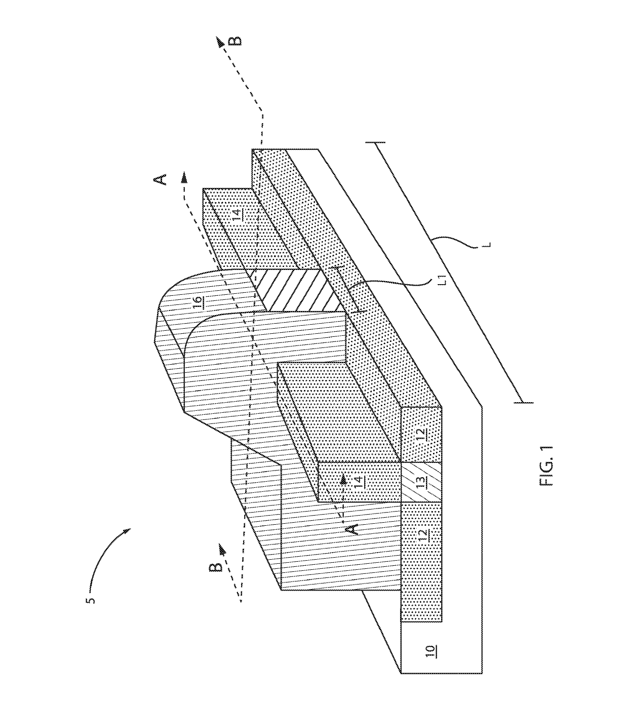
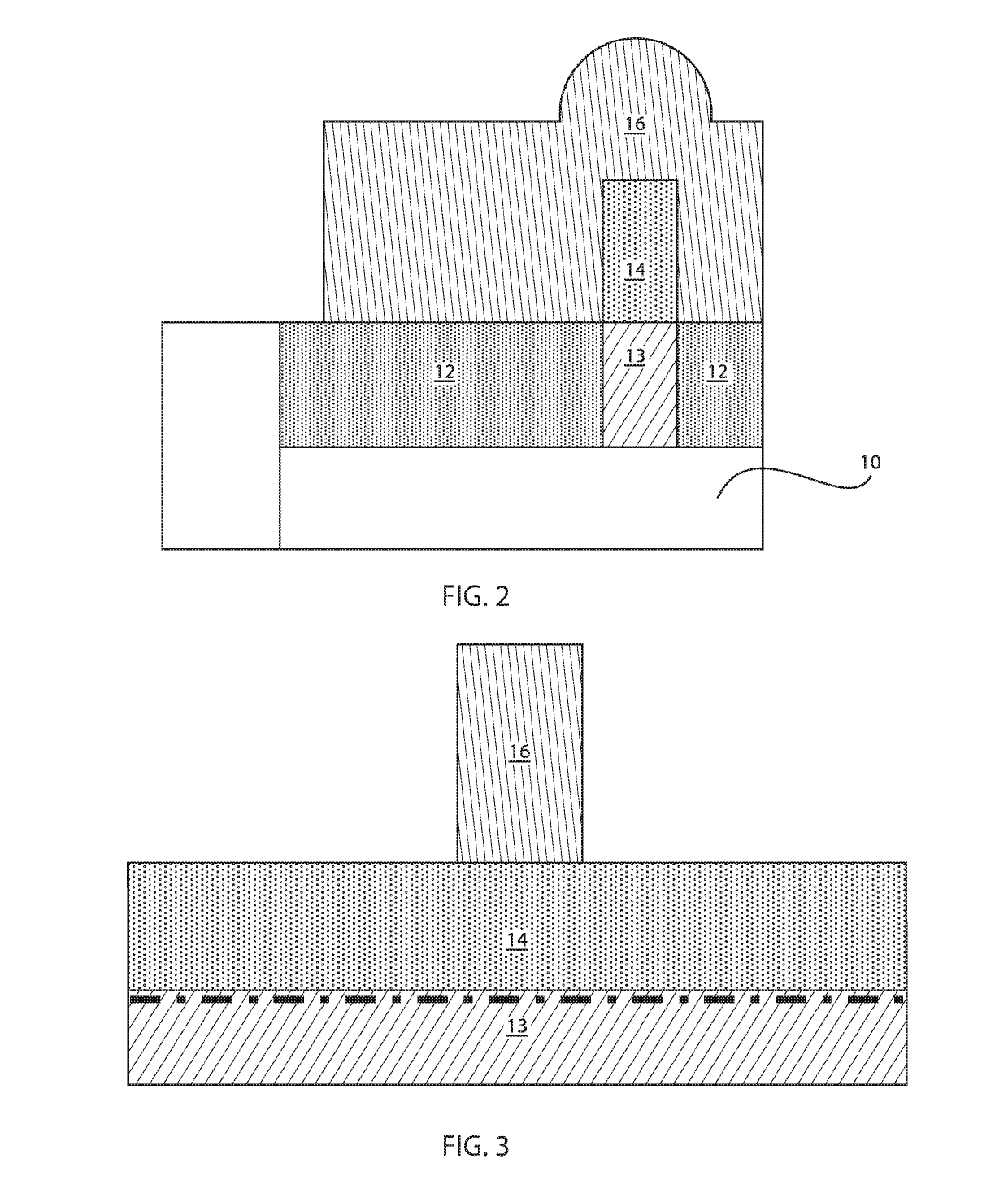
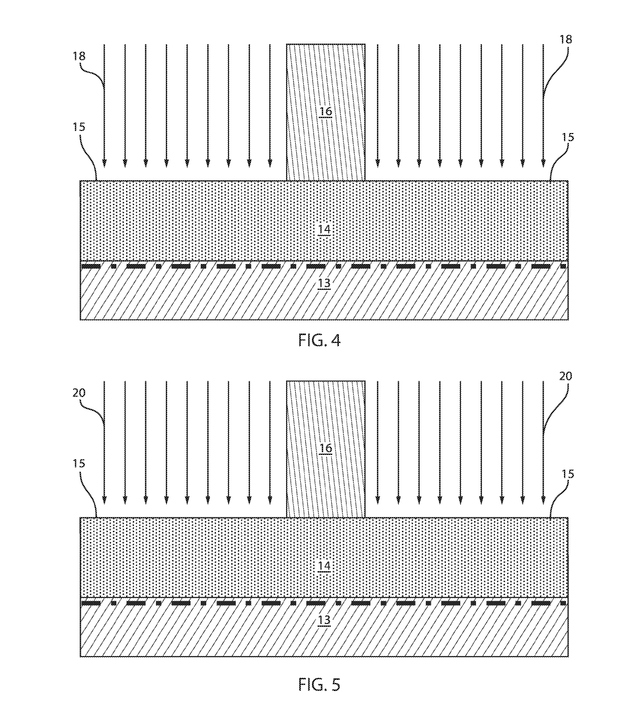
[0023]Embodiments in accordance with the present invention provide methods and devices for reducing resistance between source and / or drain regions and a channel region for a transistor. To minimize resistance in the source and / or drain regions, extension regions are doped to modify their chemical composition. In one example, the extension regions can be doped with at least two elements. The addition of such elements or dopants modifies a lattice structure of the extension region. The transistors can be, e.g., fin field effect transistors (FinFETs) or vertical field effect transistors (VFETs) or tunnel FETs or nanosheets.

[0024]Embodiments in accordance with the present invention provide methods and devices for adding or introducing or implanting gallium (Ga) and tin (Sn) to an extension region of a transistor at a temperature of about 320° C. or higher. The implantation can be implemented by, e.g., hot ion implantation techniques. For example, by adding Sn, the lattice structure of S...


PUM


Abstract

A method for reducing series resistance for transistors includes forming a conductive gate over and insulated from a semiconductor substrate, forming source and / or drain extension regions within the substrate and adjacent to respective source and / or drain regions, and forming source and / or drain regions within the substrate. The source and / or drain extension regions are formed from a material alloyed with a first dopant and a second dopant, the first dopant configured to increase a lattice structure of the material forming the source and / or drain extension regions.

Description

BACKGROUNDTechnical Field[0001]The present invention relates generally to semiconductor devices, and more specifically, to reducing series resistance between source and / or drain regions and a channel region.Description of Related Art[0002]For decades, geometrical scaling of transistor components yielded increased transistor performance and higher density at the same time. However, in a scaled-down transistor, inaccurate placement of dopants and junctions limits transistor performance. Diffused junctions and gradual dopant profiles often result in poor transistor gate control and degraded performance thus offsetting any benefit from geometrical scaling. The transistor gate control is often measured in terms of Drain Induced Barrier Lowering (DIBL) or the difference between the transistor threshold voltage measured in linear and saturation mode of operation. Abruptness of the dopant profiles and the placement of the dopant with respect to the gate edge directly control DIBL and series...

Claims


Application Information

Patent Timeline
Patent Type & Authority Patents(United States)
IPC IPC(8): H01L29/78H01L29/66H01L21/02H01L21/265H01L29/267
CPCH01L29/7845H01L21/0245H01L21/26506H01L29/7833H01L29/267H01L29/6659H01L21/26586H01L29/785H01L29/66628H01L29/66636H01L29/0847H01L29/7848H01L29/161H01L29/66795
Inventor EBRISH, MONA A.GLUSCHENKOV, OLEG
Owner INT BUSINESS MASCH CORP
Why Eureka
Try Eureka