Semiconductor device and method of manufacturing semiconductor device

a semiconductor device and semiconductor technology, applied in semiconductor devices, semiconductor/solid-state device details, electrical apparatus, etc., can solve the problems of increasing the number of terminals, narrowing the pitch between terminals, and difficult mounting of ic chips on motherboards, so as to improve yield, enable impedance control, and improve the effect of bga surface impedance control

Active Publication Date: 2019-06-25
SONY CORP
View PDF19 Cites 0 Cited by
  • Summary
  • Abstract
  • Description
  • Claims
  • Application Information

AI Technical Summary

Benefits of technology

[0030]In the above-described embodiments of the present technology, the retaining body formed on the BGA surface includes the conductive section that is formed to separate the solder balls from one another; therefore, impedance control on the BGA surface is enabled with use of the conductive section.
[0031]On that basis, in the semiconductor device according to the above-described embodiment of the present technology, the first wiring substrate having the BGA surface on which the retaining body is formed is to be connected to the circuit board; therefore, in alignment in a case where the semiconductor device is connected to the circuit board, it is only necessary to perform alignment of two components, i.e., the semiconductor device and the circuit board.
[0032]Therefore, an improvement in yields is achievable while enabling impedance control.
[0033]It is to be understood that both the foregoing general description and the following detailed description are exemplary, and are intended to provide further explanation of the technology as claimed.

Problems solved by technology

Accordingly, there has been a tendency to increase the number of terminals, thereby narrowing a pitch between terminals.
Since there is a large difference in pitch between the terminal sections in such an IC chip and connection terminals formed on a circuit board called “motherboard”, it is difficult to mount the IC chip on the motherboard.

Method used


Image

  • Semiconductor device and method of manufacturing semiconductor device
  • Semiconductor device and method of manufacturing semiconductor device
  • Semiconductor device and method of manufacturing semiconductor device

Examples


first embodiment

1. First Embodiment

1-1. Configuration of Semiconductor Device

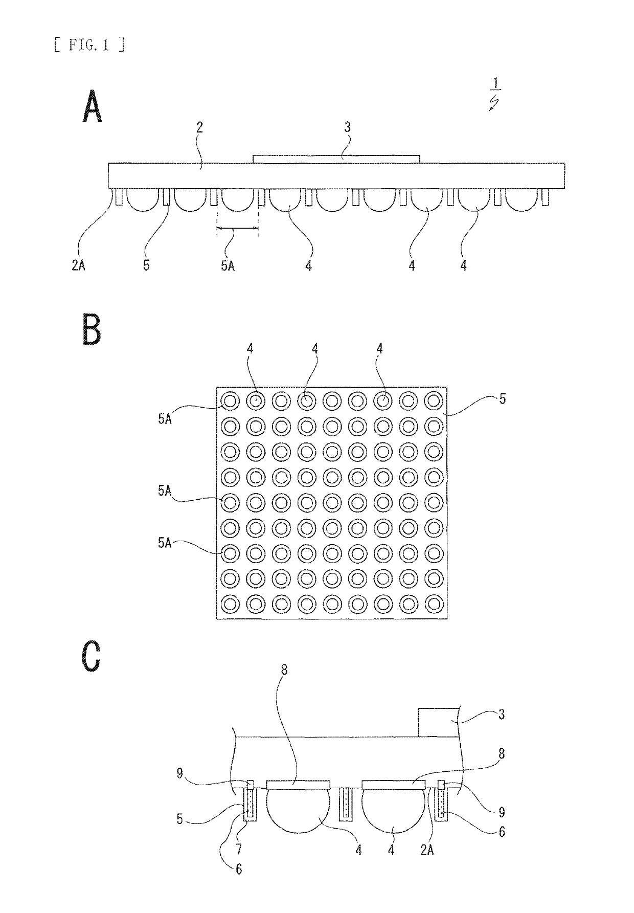
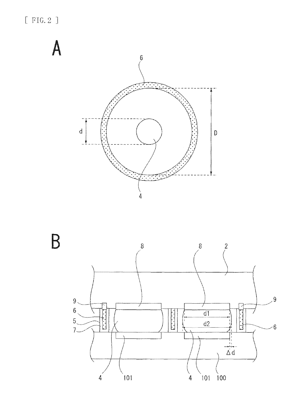
[0061]FIG. 1 is an explanatory diagram of a configuration of a semiconductor device 1 according to a first embodiment of the present technology. A of FIG. 1 is a sectional view of the semiconductor device 1, B of FIG. 1 is a bottom view of the semiconductor device 1, and C of FIG. 1 is an enlarged sectional view of a region in proximity to a BGA surface of the semiconductor device 1.

[0062]As illustrated in A of FIG. 1, the semiconductor device 1 includes a wiring substrate 2, a semiconductor chip 3, a plurality of solder balls 4, and a retaining body 5. Although not illustrated, the wiring substrate 2 is formed by alternately laminating wiring layers in which a wiring electrically connected to a predetermined terminal of the semiconductor chip 3 is formed, and insulating layers. A through hole (a via hole) is formed in each of the insulating layers, and the wirings of the respective wiring layers are connected to one anoth...

second embodiment

2. Second Embodiment

2-1. Configuration of Semiconductor Device

[0102]Next, a second embodiment will be described below.

[0103]The second embodiment relates to a semiconductor device with a PoP (Package on Package) configuration that includes, as a lower package, a semiconductor package having the BGA surface 2A for connection to the circuit board 100, as with the above-described semiconductor device 1 according to the first embodiment.

[0104]FIG. 9 is a diagram illustrating a configuration example of the semiconductor device with the PoP configuration configured by mounting (laminating), on a semiconductor package having a configuration similar to that of the semiconductor device 1, another semiconductor package.

[0105]It is to be noted that like components are denoted by like numerals as of the first embodiment and will not be further described.

[0106]In FIG. 9, a plurality of pads 12 for electrical connection to an upper package are formed on a surface (hereinafter referred to as “top ...

modification examples

3. Modification Examples

[0125]Although the present technology is described referring to the above-described embodiments, the present technology is not limited thereto. For example, as illustrated in FIG. 14, metal posts may be formed on the BGA surface 2A of the wiring substrate 2. More specifically, as illustrated in A of FIG. 14, metal posts 17 protruding from the BGA surface 2A toward a direction of connection to the circuit board 100 may be formed. These metal posts 17 may be made of, for example, copper.

[0126]In this case, the metal posts 17 are formed corresponding to the pads 8 formed on the BGA surface 2A. Then, the solder balls 4 are formed on ends of the metal posts 17.

[0127]Thus, the solder balls 4 formed on the ends of the metal posts 17 are connected to pads 101 of the circuit board 100, as illustrated in B of FIG. 14.

[0128]In this modification example, the volumes of the solder balls 4 are reduced by inserting the metal posts 17 between the pads 8 and the pads 101, the...


PUM


Abstract

A semiconductor device including a plurality of solder balls on a surface the semiconductor device, and a retaining body associated with a first solder ball of the plurality of solder balls, separating the first solder ball from at least a second solder ball of the plurality of solder balls. The retaining body includes a conductive portion and an insulating portion configured to cover the conductive portion. Also, a method of manufacturing a semiconductor device, including acts of forming a plurality of retaining bodies on a surface of a wiring substrate, each retaining body comprising a conductive portion and an insulating portion covering the conductive portion, each retaining body forming an opening section, and forming a solder ball in the opening section formed by each of the retaining bodies.

Description

CROSS REFERENCE TO RELATED APPLICATIONS[0001]This application claims the benefit of Japanese Priority Patent Application JP 2013-050141 filed Mar. 13, 2013, the entire contents which are incorporated herein by reference.TECHNICAL FIELD[0002]The present technology relates to a semiconductor device having a configuration in which a semiconductor chip is laminated on a wiring substrate and a method of manufacturing the same.CITATION LISTPatent Literature[0003][PTL 1] Japanese Unexamined Patent Application Publication No. 2002-26171[0004][PTL 2] Japanese Unexamined Patent Application Publication No. 2010-161419[0005][PTL 3] Japanese Unexamined Patent Application Publication No. H10-335547BACKGROUND ART[0006]In recent years, speed and functionality of semiconductor chips (IC (Integrated Circuit) chips) used as microprocessors of computers, cellular phones, and the like have been enhanced more and more. Accordingly, there has been a tendency to increase the number of terminals, thereby na...

Claims


Application Information

Patent Timeline
Patent Type & Authority Patents(United States)
IPC IPC(8): H01L23/498H01L21/48H01L25/10H01L23/00H01L23/66
CPCH01L23/49816H01L21/4853H01L21/4857H01L23/49822H01L23/49838H01L24/17H01L25/105H01L2924/15331H01L2924/15311H01L2924/15192H01L2924/1517H01L2924/1511H01L2924/152H01L2924/1436H01L2225/1058H01L23/66H01L24/16H01L24/32H01L24/73H01L2223/6622H01L2224/16225H01L2224/16227H01L2224/32225H01L2224/73204H01L2225/1023H01L2924/00012H01L2924/00
Inventor HAREYAMA, KOSUKECHINO, DAISUKENISHITANI, YUUJI
Owner SONY CORP
Why Eureka
Try Eureka