Semiconductor device

a technology of semiconductor devices and semiconductors, applied in the field of semiconductor devices, can solve the problems of weakened (or deteriorated) implants at high energy, the reliability of semiconductor devices according to the related art is low, and the insulating film zmb>2/b> is more difficult to be polished than the insulating film, so as to achieve the effect of improving the reliability of semiconductor devices

Active Publication Date: 2019-07-02
RENESAS ELECTRONICS CORP
View PDF9 Cites 0 Cited by
  • Summary
  • Abstract
  • Description
  • Claims
  • Application Information

AI Technical Summary

Benefits of technology

[0005]It is desired to improve reliability of a semiconductor device produced by using an SOI substrate.
[0008]According to an embodiment, the reliability of the semiconductor device can be improved.

Problems solved by technology

More specifically, it has been found that the reliability of the semiconductor device according to the related art is low.
However, this case causes such a disadvantage as increase in an area of the semiconductor device.
More specifically, the polishing process is performed under a condition under which the insulating film ZM2 is more difficult to be polished than the insulating film.
Furthermore, this is because the silicon oxide film constituting the element isolation region STI in the region to which the phosphorus ions or the arsenic ions having the relatively large mass have been ion-implanted at the high energy is weakened (or deteriorated) and is easily etched by the above-described etchant.

Method used


Image

  • Semiconductor device
  • Semiconductor device
  • Semiconductor device

Examples


first embodiment

Main Features of Present First Embodiment

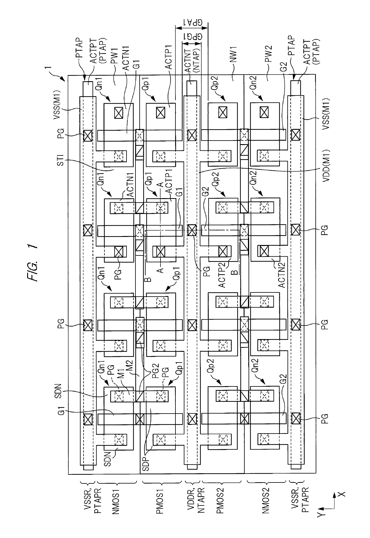
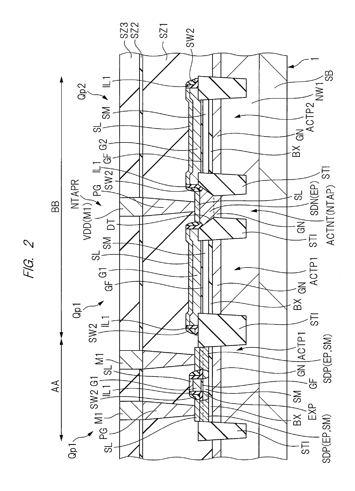
[0117]In the n-type tap region NTAPR, the epitaxial layer EP is not formed on the main surface of the n-type well region NW1 (i.e., the semiconductor substrate SB). More specifically, the embodiment has such a feature that the lower surface of the silicide layer SL in the active region ACTNT of the n-type tap region NTAPR is lower by d1 than the lower surface of the insulating layer BX in the active region ACTP1 which is the formation region of the p-type MISFET Qp1 (closer to the back surface of the semiconductor substrate SB). This feature can prevent the short circuit or the breakdown voltage deterioration between the n-type well region NW1 and the gate electrodes G1 or G2 of the p-type MISFET Qp1 close to the n-type tap region NTAPR.

[0118]In the p-type tap region PTAPR, the epitaxial layer EP is formed on the main surface of the p-type well region PW1 (i.e., the semiconductor substrate SB). More specifically, the embodiment has such a fea...

second embodiment

[0119]The present second embodiment is a modification example of the first embodiment, and only differences from the first embodiment will be explained. FIG. 19 is a plan view of a semiconductor device according to the present second embodiment. FIG. 20 is a detailed plan view of the part B of FIG. 19. FIG. 21 is a cross-sectional view taken along a line G-G, a line H-H, a line I-I, a line J-J, a line K-K, and a line L-L of FIG. 20. In FIG. 21, a cross-sectional view along the line G-G of FIG. 20 is shown in a region GG, a cross-sectional view along the line H-H of FIG. 20 is shown in a region HH, a cross-sectional view along the line I-I of FIG. 20 is shown in a region II, a cross-sectional view along the line J-J of FIG. 20 is shown in a region JJ, a cross-sectional view along the line K-K of FIG. 20 is shown in a region KK, and a cross-sectional view along the line L-L of FIG. 20 is shown in a region LL. FIG. is a cross-sectional view in a step of manufacturing the semiconductor ...

third embodiment

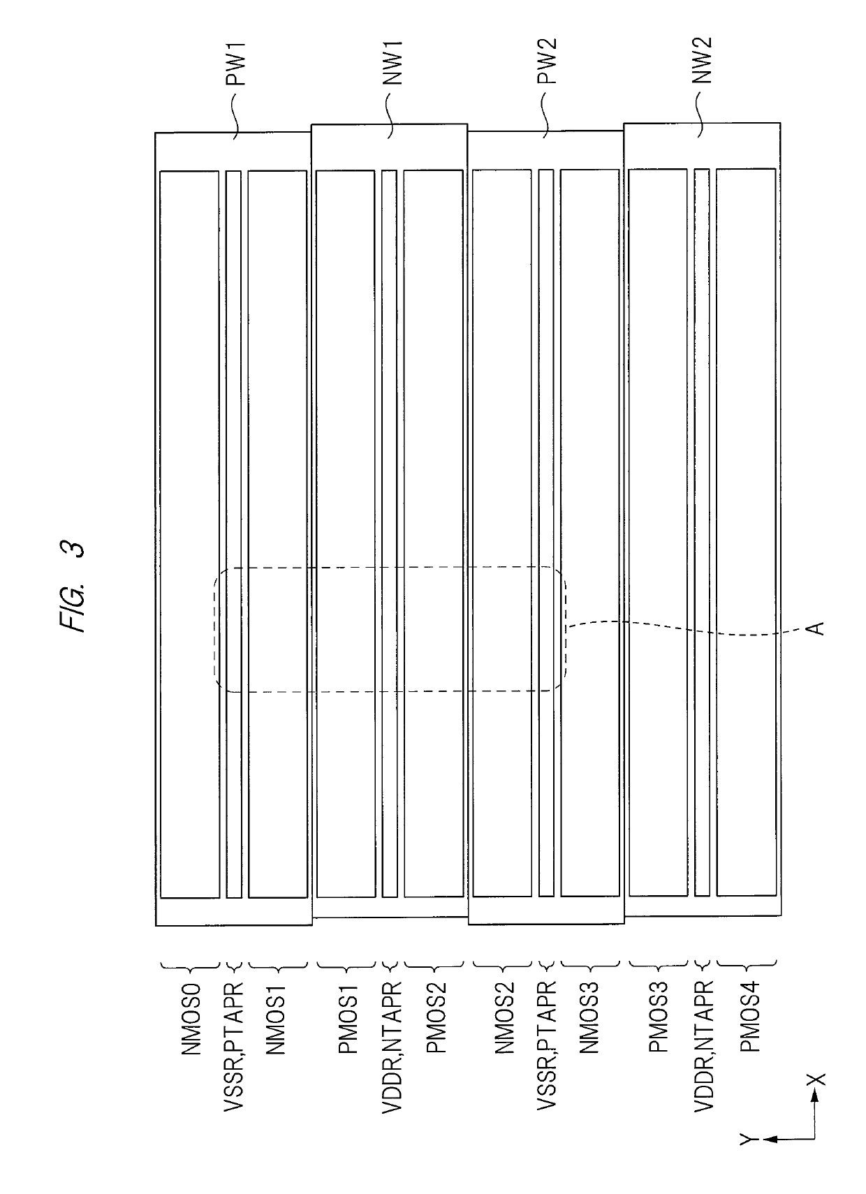
[0140]FIG. 23 is a plan view of a semiconductor device according to the present third embodiment.

[0141]As shown in FIG. 23, the semiconductor device according to the present third embodiment uses the structure of the first embodiment for the NMOS regions NMOS0 to NMOS3 and the p-type tap region PTAPR in the p-type wells PW1 and PW2, and uses the structure of the second embodiment for the PMOS regions PMOS1 to PMOS4 and the n-type tap region NTAPR1 in the n-type well regions NW1 and NW2. More specifically, the structure of the second embodiment can be employed only for a portion that is largely affected by the dent DT of the element isolation region STI. As a result, the flexibility of the layout design can be increased.


PUM


Abstract

Reliability of a semiconductor device is improved. A p-type MISFET of a thin film SOI type is formed in an SOI substrate including a semiconductor substrate, an insulating layer on the semiconductor substrate, and a semiconductor layer on the insulating layer, and n+-type semiconductor regions which are source and drain region of the p-type MISFET are formed in the semiconductor layer and an epitaxial layer on the semiconductor layer. A semiconductor layer is formed via the insulating layer below the p-type MISFET formed in the n-type well region of the semiconductor substrate. In an n-type tap region which is a power supply region of the n-type well region, a silicide layer is formed on a main surface of the n-type well region without interposing the epitaxial layer therebetween.

Description

CROSS-REFERENCE TO RELATED APPLICATION[0001]The present application claims priority from Japanese Patent Application No. 2016-222054 filed on Nov. 15, 2016, the content of which is hereby incorporated by reference into this application.TECHNICAL FIELD OF THE INVENTION[0002]The present invention relates to a semiconductor device. For example, the present invention can be suitably used for a semiconductor device using an SOI substrate.BACKGROUND OF THE INVENTION[0003]In order to produce a semiconductor device, an element isolation region is formed in a semiconductor substrate, and a semiconductor element such as a MISFET (Metal Insulator Semiconductor Field Effect Transistor) is formed in an active region of a semiconductor substrate defined by the element isolation region, and a multilayer wiring structure is formed on the semiconductor substrate. Also, there is a technique using an SOI substrate as a semiconductor substrate.[0004]Japanese Patent Application Laid-Open Publication No....

Claims


Application Information

Patent Timeline
Patent Type & Authority Patents(United States)
IPC IPC(8): H01L21/8238H01L27/02H01L29/417H01L29/78H01L27/12G05F1/625H03K17/687H01L21/84
CPCH01L27/1203G05F1/625H01L27/02H01L27/0207H01L27/1244H01L29/78H03K17/687H01L29/41733H01L21/84H01L21/8238H01L21/823871H01L21/823481H01L27/088H01L29/665H01L29/42312H01L29/6656H01L21/7624
Inventor TSUBOI, NOBUOYAMAMOTO, YOSHIKI
Owner RENESAS ELECTRONICS CORP
Why Eureka
Try Eureka