
Eureka
For R&D, Eureka makes reading and utilizing patents & technical documents easy.
Eureka AIR
Designed for self-driven R&D workflows. Generate viable solutions, solve complex R&D challenges, empower your innovation with AI.

Eureka Materials
Designed for material experts only. Revolutionize your material R&D, from search, analyze, to developing new materials.

TechResearch
Generate reliable direction feasibility study reports for your R&D in just a few steps.

TechSeek
Discover and master advanced knowledge NOW. Basics, ideas, possibilities, all at once.

TechMind
As an expert in R&D Theories, TechMind can generates customized viable solutions instantly.

TechRisk
Analyze your overall solution with one click, know your potential R&D risks in advance.

TechMonitor
Get weekly tech updates, stay abreast of the latest tech innovations and key insights.
Hot swap control circuit and related storage server system
- Summary
- Abstract
- Description
- Claims
- Application Information
AI Technical Summary
Benefits of technology
Problems solved by technology
Method used
Image

Examples
Embodiment Construction
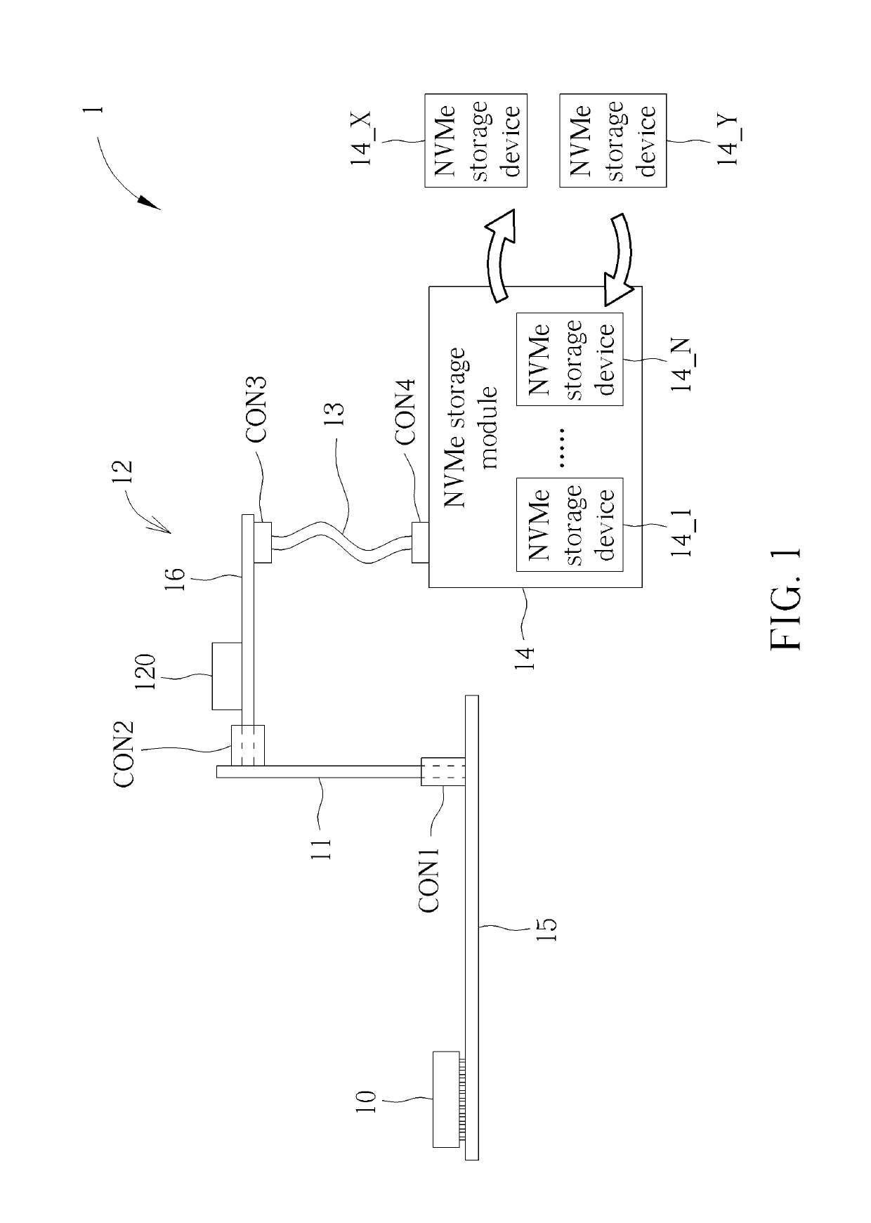
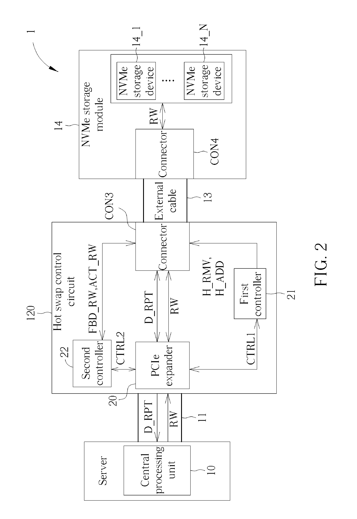
[0015]FIG. 1 is a schematic diagram of a storage server system 1 according to an embodiment of the present invention. The storage server system 1 includes a central processing unit (or a storage server) 10, a riser card 11, a switch card 12, an external cable 13, a Non-Volatile Memory Express (abbreviated NVMe) storage module 14 and a main board 15. A central processing unit 10 and a connector CON1 are disposed on the main board 15. The riser card 11 includes a connector CON2. The switch card 12 includes a substrate 16, a connector CON3 and a hot swap control circuit 120, wherein the connector CON2 and the hot swap control circuit 120 are disposed on the substrate 16. The NVMe storage module 14 includes multiple NVMe storage devices 14_1-14_N and a connector CON4.
[0016]The riser card 11 may be inserted into the connector CON1 to connect to the main board 15, and connect to central processing unit 10 through the main board 15. The switch card 12 may be inserted into the connector CON...
PUM
 Abstract
Description
Claims
Application Information
 - R&D Engineer
- R&D Manager
- IP Professional
- Industry Leading Data Capabilities
- Powerful AI technology
- Patent DNA Extraction
Browse by: Latest US Patents, China's latest patents, Technical Efficacy Thesaurus, Application Domain, Technology Topic, Popular Technical Reports.
© 2024 PatSnap. All rights reserved.Legal|Privacy policy|Modern Slavery Act Transparency Statement|Sitemap|About US| Contact US: help@patsnap.com