Integrated metal layer aware optimization of integrated circuit designs

a technology of integrated circuit design and integrated metal layer, applied in the field of integrated circuits, can solve the problems of long runtimes of existing ic design tools and ic design flows, rapid increase in the size and complexity of ic designs, and poor quality

Active Publication Date: 2019-07-23
SYNOPSYS INC
View PDF26 Cites 2 Cited by
  • Summary
  • Abstract
  • Description
  • Claims
  • Application Information

AI Technical Summary

Problems solved by technology

Advances in process technology and an almost unlimited appetite for consumer electronics have fueled a rapid increase in the size and complexity of IC designs.
Existing IC design tools and IC design flows can have long runtimes and / or poor quality of results (QoR).

Method used


Image

  • Integrated metal layer aware optimization of integrated circuit designs
  • Integrated metal layer aware optimization of integrated circuit designs
  • Integrated metal layer aware optimization of integrated circuit designs

Examples


Embodiment Construction

[0015]The following description is presented to enable any person skilled in the art to make and use the invention, and is provided in the context of a particular application and its requirements. Various modifications to the disclosed embodiments will be readily apparent to those skilled in the art, and the general principles defined herein may be applied to other embodiments and applications without departing from the spirit and scope of the present invention. Thus, the present invention is not limited to the embodiments shown, but is to be accorded the widest scope consistent with the principles and features disclosed herein.

Overview of IC Design and Manufacturing

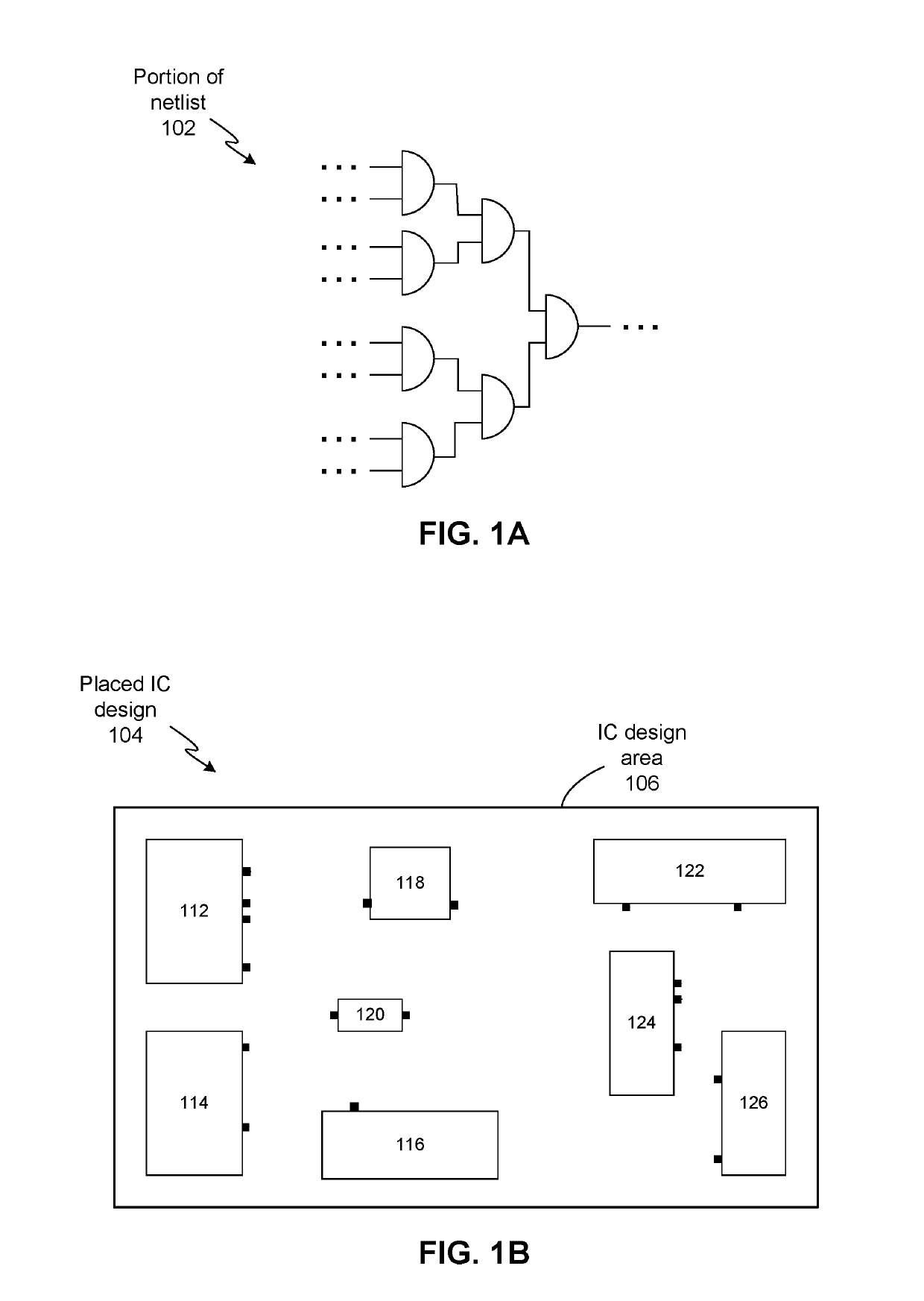
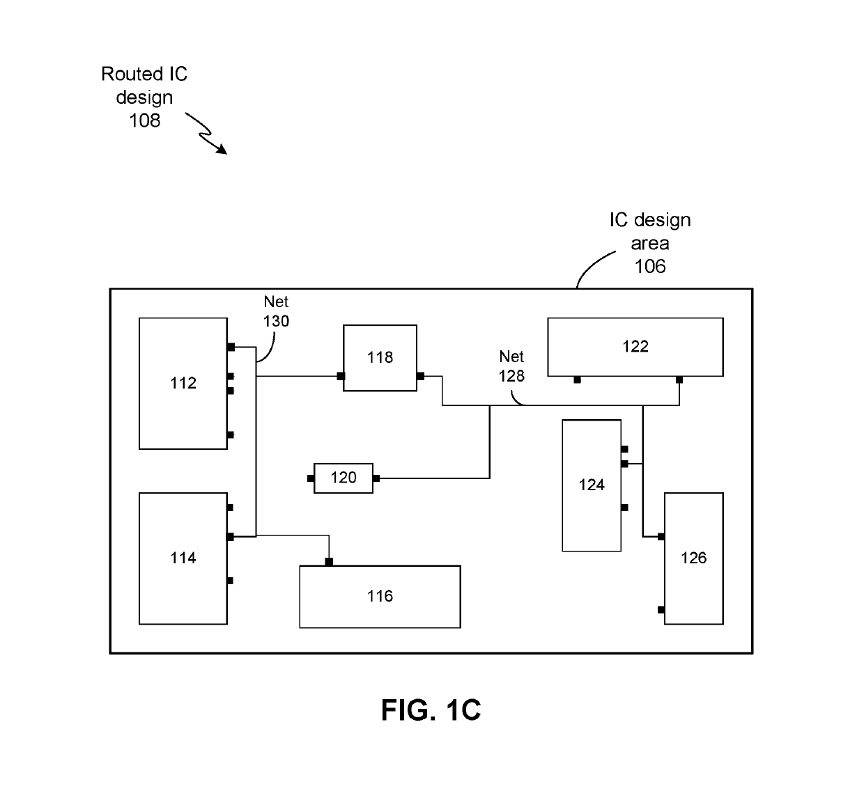
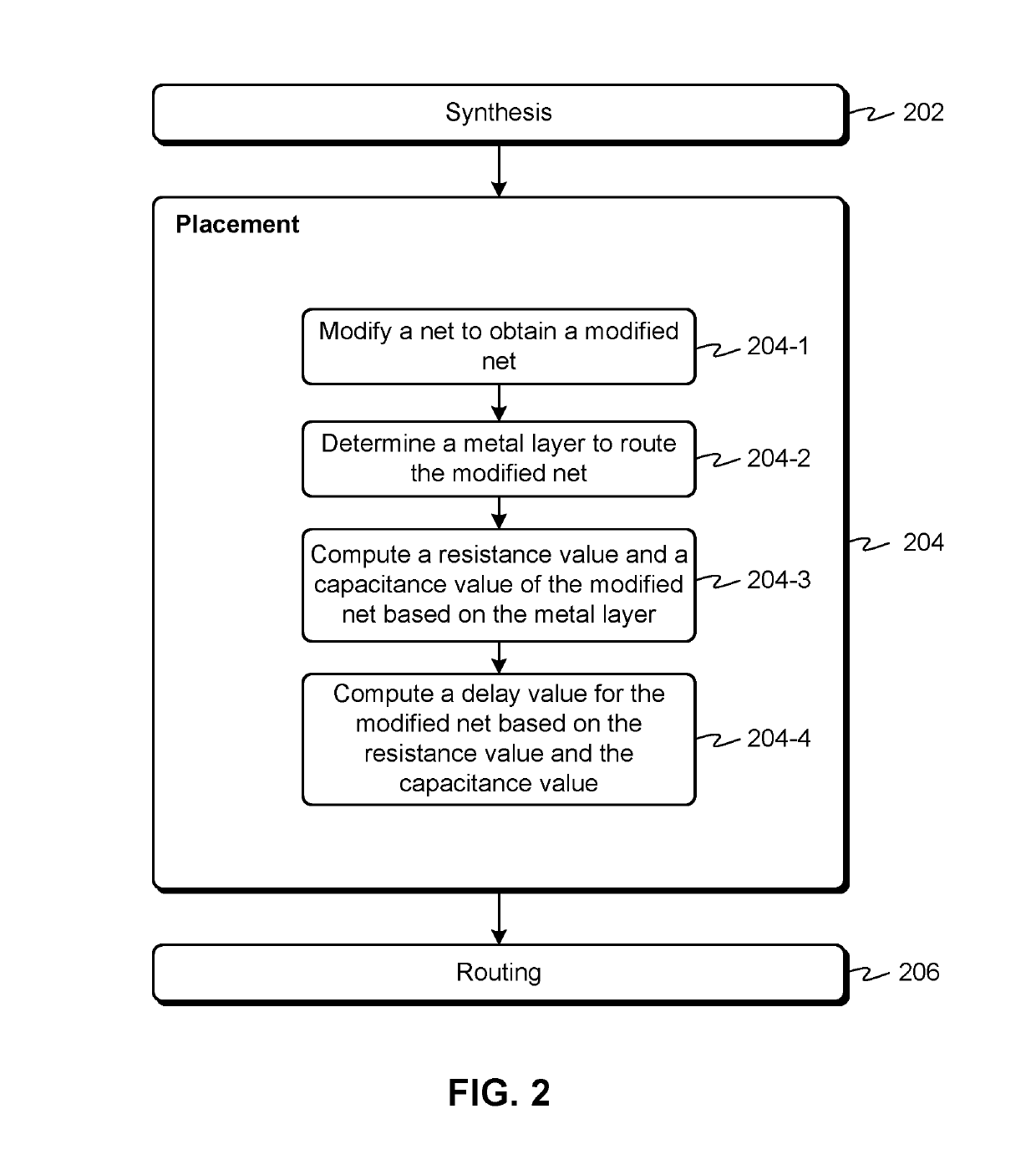
[0016]IC design software tools can be used to create an IC design. Once the IC design is finalized, it can undergo fabrication, packaging, and assembly to produce IC chips. The overall IC design and manufacturing process can involve multiple entities, e.g., one company may create the software for designing ICs, another c...


PUM


Abstract

Systems and techniques are described for optimizing an integrated circuit (IC) design. Before routing is performed on the IC design in an IC design flow, an IC design tool can iteratively perform a set of operations, the set of operations comprising: (1) modifying a net in the IC design to obtain a modified net, (2) determining a metal layer for routing the modified net, (3) computing a resistance value and a capacitance value of the modified net based on the metal layer, and (4) computing a delay value for the modified net based on the resistance value and the capacitance value.

Description

TECHNICAL FIELD[0001]This disclosure relates to integrated circuits (ICs). More specifically, this disclosure relates to techniques and systems for integrated metal layer aware optimization of integrated circuit designs.BACKGROUNDRelated Art[0002]Advances in process technology and an almost unlimited appetite for consumer electronics have fueled a rapid increase in the size and complexity of IC designs. Existing IC design tools and IC design flows can have long runtimes and / or poor quality of results (QoR).SUMMARY[0003]Some embodiments described herein provide techniques and systems for optimizing an IC design before routing is performed on the IC design in an IC design flow. During synthesis or pre-route optimization (these steps are performed before routing), an IC design tool can iteratively perform a set of optimization operations to minimize (1) a delay objective function for the IC design, (2) an area objective function for the IC design, and / or (3) a leakage power objective f...

Claims


Application Information

Patent Timeline
Patent Type & Authority Patents(United States)
IPC IPC(8): G06F17/50
CPCG06F17/5081G06F17/5077G06F17/5072G06F2217/84G06F30/39G06F30/392G06F30/394G06F30/398G06F2119/12
Inventor CHAKRABORTY, ABHIJEETSEIBERT, DAVID JOHNFOK, PINGKANRAO, RAMOJI KARUMURI
Owner SYNOPSYS INC
Why Eureka
Try Eureka