Precision spray processes for direct write electronic components

a technology of electronic components and spray processes, applied in the direction of 3d object support structures, chemical vapor deposition coatings, conductive pattern formation, etc., can solve the problems of limiting the operation of cladding, and reducing the size of the circuit board, etc., to achieve increased flight time, high reflection, and long flight path

Inactive Publication Date: 2001-06-26
OPTOMEC DESIGN CO
View PDF14 Cites 417 Cited by
  • Summary
  • Abstract
  • Description
  • Claims
  • Application Information

AI Technical Summary

Benefits of technology

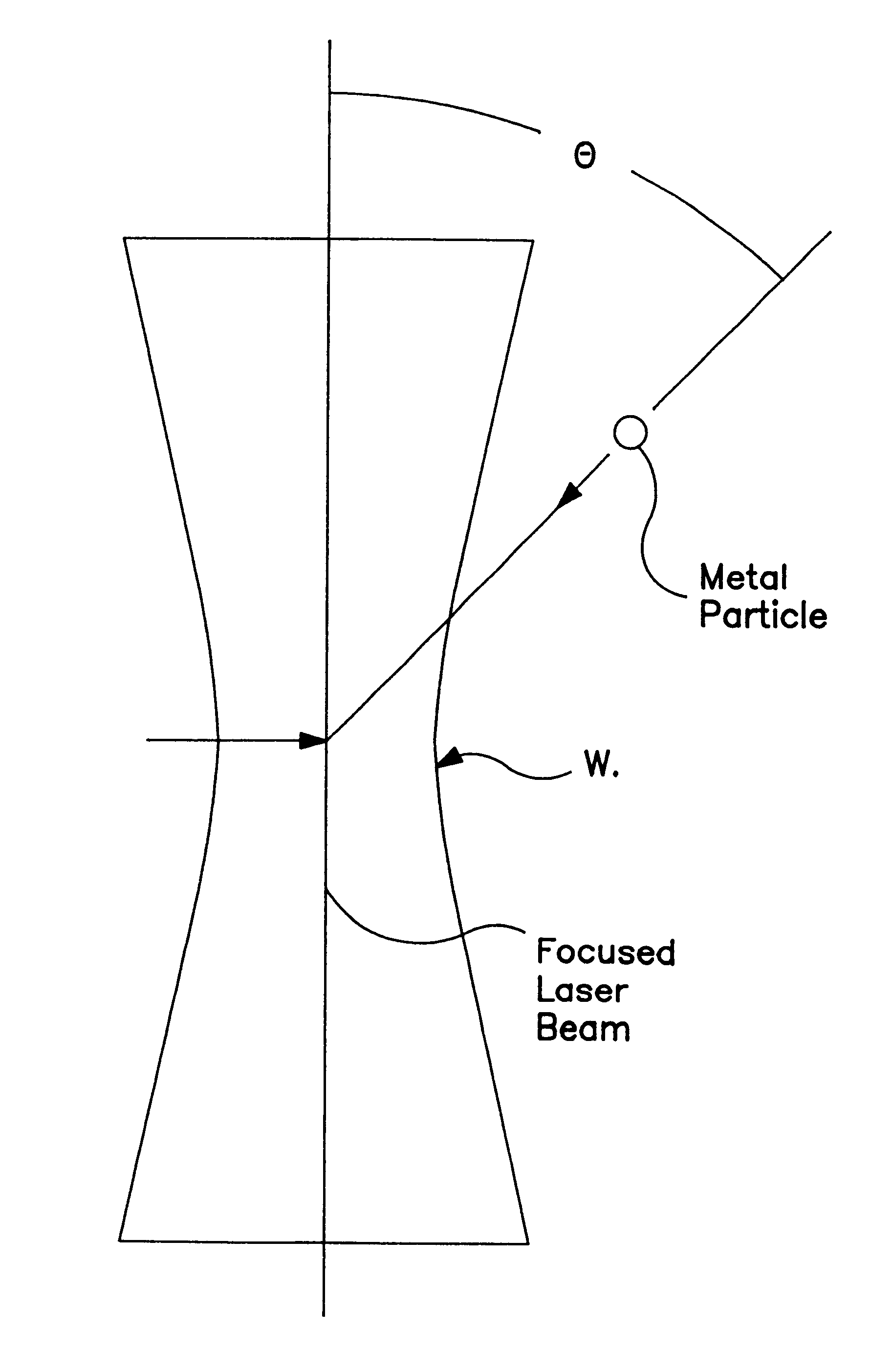
The laser beam intersection region 15 shown in FIG. 5 provides an advantage that comes from a longer time of flight path for feedstock material in elliptically focused laser beams. Many of powdered feedstock materials can be highly reflective with only a small fraction of the incident laser energy being absorbed into a particle. As such, a high percentage of the laser power incident onto a particle may be reflected and therefor rendered unavailable to the particle from which it was reflected. This energy is, however, available to other particles that are in the path of the reflected beams. The elliptical beam cross-section provides an increased time of flight for the particles within the laser beam intersection region 15 and, as such, increases the probability that the reflected energy will be incident onto, and subsequently absorbed into neighboring powder particles within the focused beams.
This method will also greatly reduce the use or even eliminate the need to create a molten puddle on the substrate surface. This broadens the range of materials that can be used as deposition substrates. Ceramics and other materials susceptible to thermal shocking due to the large thermal gradient created during the laser aided material deposition process are now candidate materials for use in the practice of the present invention. This technology now approximates a thermal spray process in which energy is stored in molten particles that can be directed onto a broad range of materials without damaging these substrates.
Another advantage offered by the practice of the present invention comes in the form of reduced residual stress contained within the fabricated structures. Laser assisted material deposition processes that rely on substrate melting to cause particles to melt impart sufficient heat into the substrate to cause even thick substrates to be distorted. This effect is reduced as the energy input to the substrate material is reduced. Eliminating the bulk melting characteristics of these processes will significantly reduce this stress. In addition, the impacting characteristics of the depositable particle will behave similarly to thermal spray processes in which shrinkage of the substrate surface is counteracted by outward force due to the particle droplet spreading on impact. In accordance with the present invention, it has been observed that partially melted particles adhere to the surface of components fabricated using current laser assisted material deposition processes. It has also been shown that the particle diameter plays a significant role in the final surface finish of a deposited structure. Since these fine-sized particle materials are typically an order of magnitude smaller in diameter than the materials used in prior art laser assisted material deposition processes; the surface finish due to particle adhesion will be much better.
The present invention can be employed in a number of applications including, for example, the field of flip-chip technology. As packaging size continues to shrink, it is increasingly difficult to apply solder to the points of interconnection. Although solder jetting technologies will work for some intermediate size electronics packages, the direct deposition of solder onto small interconnects is crucial to further miniaturization of packaging. When used for the direct application of solder to interconnects, the present invention will allow solder to be applied to a very small area (on the order of microns). One configuration for flip-chip packages is an array of interconnects located on the bottom of the package. The present invention can be used to apply solder feedstock material to the connectors. In this application, the solder can be provided in finely divided powder form. The solder particles thus provided are very small as compared to the connector pads to which they are to be applied, thereby allowing the connector pad to be considerably reduced in size compared to existing technology. The application of solder bumps that are less than 50 .mu.m in diameter is achievable with the present invention; as a result the potential exists to significantly increase the packaging density available for microelectronic applications.
Yet another application of the present invention is in the repair of existing electrical hardware such as, for example, flat panel displays, printed circuit for microelectronics, and the like. For the repair application, there may be an existing circuit that has a high value associated with it and yet due to incomplete processing or another event, a flaw is present in the conductor traces. This could be, for example, as shown in FIG. 4b in the lower portion of the conductor patterns where there are discontinuous lines. If, in fact, these lines were meant to be connected, the component, as depicted, would be defective. The present invention provides the opportunity to allow the high value component to be saved by depositing a conductive material in a specific pattern between the disconnected conductors such that they become electrically connected.

Problems solved by technology

Although the IC industry has gone through revolutionary changes in packing density and device performance, the electronics packaging industry has not seen the same degree of size reduction.
Since each of the discrete devices must be placed onto the circuit board and bonded in place, various physical constraints dictate the size that the circuit board must maintain.
Due to the relatively high heat input and localized heating of laser cladding processes, the cladding operation is primarily limited to more ductile metallic materials.
When this process is applied to materials that are sensitive to thermal shock, catastrophic failure of the deposited material or substrate materials generally occurs.
However, the use of a laser to melt the substrate creates excessive heat in the part, causing distortion and residual stress within the part being made.
Also, the high energy level required of a laser suitable for this method causes inefficiencies throughout the system.
One of the limitations of the thermal spray process is in its lack of ability to produce fine features, such as those produced by laser cladding processes.
The use of nozzles in thermal / plasma spray processes has added certain advantages to these processes; however, the disadvantage of inability to produce fine features remains.
However, this system relies solely on the use of a laser created plasma to melt the particles before they are ever introduced to the deposition region.
This design provides a unique method for coating parts; however, it has never been intended for fabrication of multi-layered parts.
Due to the diverging nature of the powder material, this plasma technique fails to provide the feature definition necessary for fabricating complex, net-shaped objects.
Although this resolution is adequate for large area deposition, it is inadequate for precision deposition applications.
In fact, this process is essentially limited to CO.sub.2 and CO lasers since these lasers are the only sources currently available which can generate these power levels.
These lasers are very expensive and, as a result, limit application of this method.

Method used


Image

  • Precision spray processes for direct write electronic components
  • Precision spray processes for direct write electronic components
  • Precision spray processes for direct write electronic components

Examples


Embodiment Construction

There are numerous processing sequences that could effectively be used to create the direct write circuitry contemplated by invention methods. Based on the layout shown in FIG. 3, each of these devices, as well as the conductive lines 26, can be produced using a sequence of steps. An exemplary, albeit basic methodology for sequencing the process to create the circuitry of FIG. 3 is shown in FIGS. 4A-G.

In FIG. 4A, the test substrate 10 is shown with only a resistive material pattern 24a applied to the substrate. After the resistive material is applied, the process can be sequenced to then apply a conductive material. The conductive material is usually a metallic material and is used in essentially all of the components.

As shown in FIG. 4B, the conductive lines 26 are deposited in the desired pattern. A conductive material is also used to deposit the lower conductive pattern 38a for each of the capacitors, the lower coil conductor pattern 32a that serves to form the bottom half of the...


PUM

PropertyMeasurementUnit
diameteraaaaaaaaaa
distanceaaaaaaaaaa
poweraaaaaaaaaa

Abstract

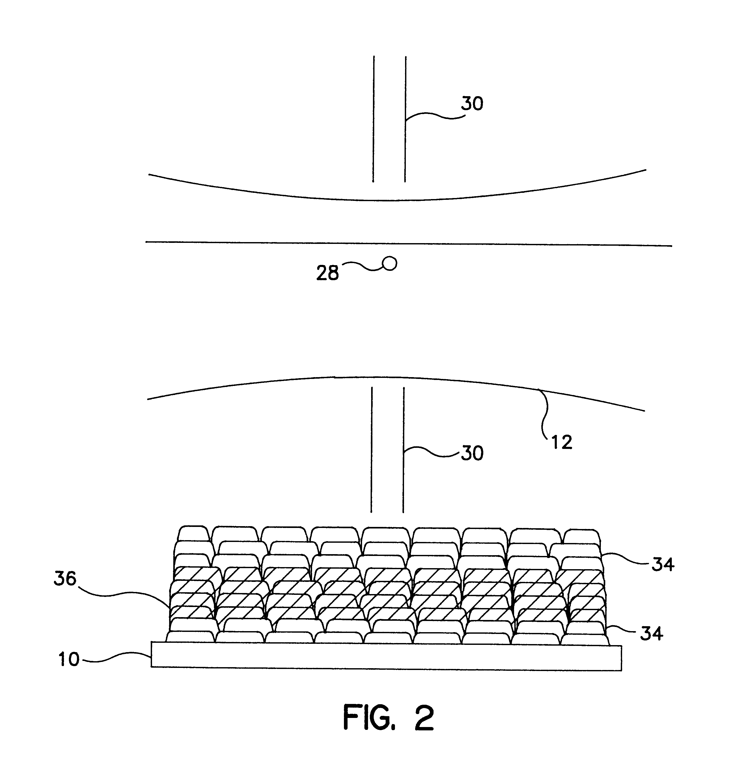
This invention combines the precision spray process with in-flight laser treatment in order to produce direct write electronic components. In addition to these components, the process can lay down lines of conductive, inductive, and resistive materials. This development has the potential to change the approach to electronics packaging. This process is revolutionary in that components can be directly produced on small structures, thus removing the need for printed circuit boards.

Description

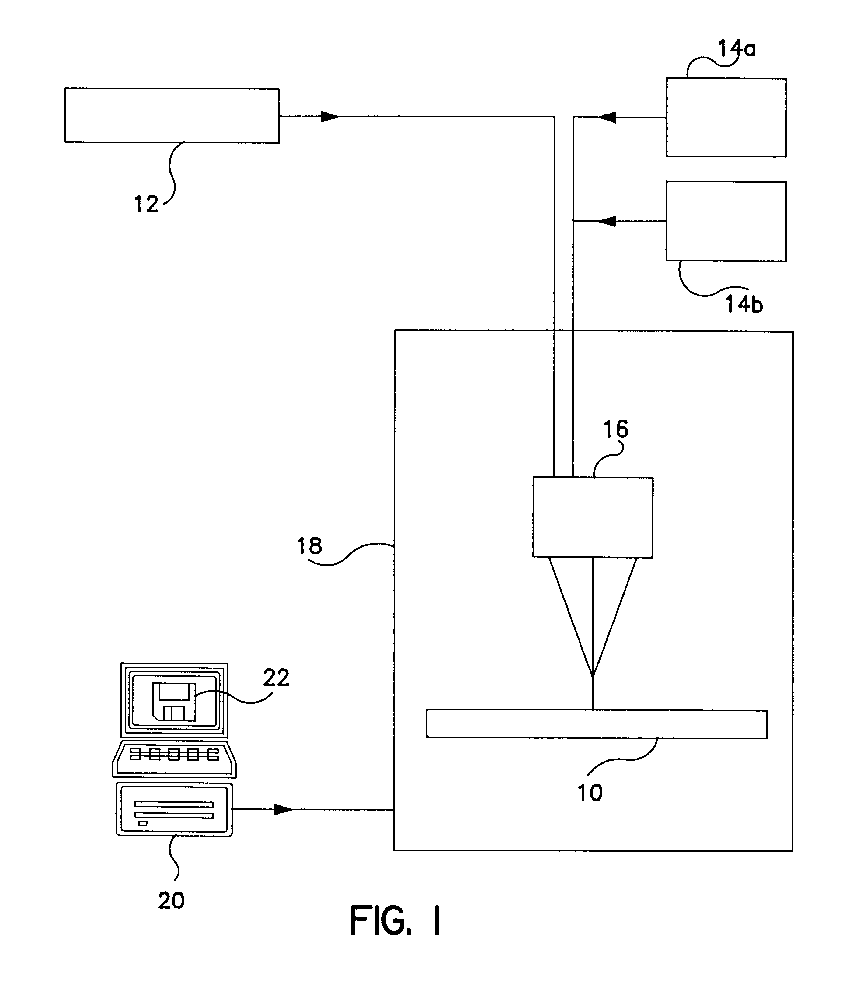
This invention combines precision spray processes with in-flight laser treatment in order to produce direct write electronic components and for other direct material applications. Apparatus for performing invention processes are also provided.Recent developments in the microelectronics industry have allowed commercial integrated circuit (IC) chip manufacturers to achieve a very high packing density within a single IC chip. Submicron features can now be produced on a regular basis. Although the IC industry has gone through revolutionary changes in packing density and device performance, the electronics packaging industry has not seen the same degree of size reduction. One reason for this difference lies in the need to use discrete passive and active electronic devices on circuit boards as well as electrical interconnections to obtain fully functioning IC devices. Since each of the discrete devices must be placed onto the circuit board and bonded in place, various physical constraints...

Claims


Application Information

Patent Timeline
Patent Type & Authority Patents(United States)
IPC IPC(8): B23K26/00B23K26/34B29C67/00H01L21/02H01L21/48H01L21/3213H05K3/10H05K3/46C23C4/12H01L21/285H01L21/3205H01L21/82H01L21/822H01L27/04
CPCB23K26/34B29C67/0077B29C67/0092H01L21/32131H01L21/481H01L21/4846H05K3/102B23K26/3206B23K26/3246B23K26/3266B23K26/3273B23K26/328B23K35/0244H05K3/4664H05K2203/107H05K2203/1344B23K26/32B23K26/324B29C64/153B29C64/40B23K2103/16B23K2103/172B23K2103/30B23K2103/50B23K2103/52
Inventor MILLER, W. DOYLEKEICHER, DAVID M.ESSIEN, MARCELINO
Owner OPTOMEC DESIGN CO
Why Eureka
Try Eureka