Semiconductor device and electric apparatus using same

a technology of semiconductor devices and electrodes, applied in the direction of semiconductor devices, electrical devices, basic electric elements, etc., can solve the problems of difficult to achieve epitaxial growth of monocrystals, limited substrate selection, and difficult to use, etc., to reduce backward leak current, and use schottky electrodes easy

Active Publication Date: 2019-08-06
IDEMITSU KOSAN CO LTD
View PDF10 Cites 1 Cited by
  • Summary
  • Abstract
  • Description
  • Claims
  • Application Information

AI Technical Summary

Benefits of technology

[0094]When the n is excessively low, there are risks that a trap which is present in the semiconductor layer might have an influence to increase contribution of a diffusion current and the current characteristics might deteriorate. On the other hand, when the n has a value of εVe / qL2 or more in the formula (I), contribution of a drift current increases, and behavior characteristics come close to conventional behavior characteristics to hardly produce the effect of the invention.
[0096]The semiconductor device of the invention comprises a semiconductor layer between a pair of an ohmic electrode and a Schottky electrode. As compared with the conventional power device, a designed carrier concentration is lower, and hence a designed withstand voltage VBD is from VBD to EcL, whereas a conventional withstand voltage is from VBD to ECL / 2. In comparison with the conventional power device having the same L, it can be expected that the withstand voltage increases as much as about two times. Here, the Ec is a maximum dielectric breakdown field and the L is a length between the electrodes.
[0097]Furthermore, in the conventional power device, the initial carrier concentration is high, and hence when a reverse bias is applied, a leak current is large. Additionally, it is difficult to take a device configuration where, when vertical lines are drawn from an outer periphery (a side surface) of a surface of the Schottky electrode toward the surface of the ohmic electrode, the surface of the ohmic electrode is present inside the vertical lines from the surface of the Schottky electrode. In the invention, the initial carrier concentration in the semiconductor layer is low, and when a forward voltage is applied, the external carrier is injected only into a range where, when vertical lines are drawn from the outer periphery of a surface of the Schottky electrode toward the surface of the ohmic electrode, the surface of the ohmic electrode is present inside the vertical lines from the periphery of a surface of the Schottky electrode. On the other hand, when the reverse bias is applied, there is less influence of leakage of a current which flows around, because the carrier is not present over the whole semiconductor layer.
[0098]FIG. 5 is a view to explain an electrode surface of the semiconductor device in FIG. 2. In FIG. 5, the outer periphery of a surface of the Schottky electrode is a part denoted with numeral 12, and the surface of the ohmic electrode is a part denoted with numeral 22. The vertical lines drawn from the outer periphery 12 of a surface of the Schottky electrode toward the surface 22 of the ohmic electrode are denoted with character A.
[0099]In a vertical type power device, a lower part of the semiconductor layer usually forms the ohmic electrode, but when the ohmic electrode is present inside the vertical lines from the Schottky electrode, it is possible to easily use the Schottky electrode in the lower part of the semiconductor layer. Furthermore, it is known that in a usual power device, decrease of the backward leak current is achieved by using an electric field relaxing structure of a guard ring or the like, and by use of this configuration, it is possible to omit or reduce the electric field relaxing structure which has been a process demerit.
[0100]In the uni-polar type power device in which the external carrier is dominant, the withstand voltage is from VBD to EcL as described above, and hence the dielectric breakdown field can easily be determined from measurement results of the length L between the electrodes and the withstand voltage VBD. Here, the withstand voltage per L corresponds to the dielectric breakdown field. When the withstand voltage per film thickness is high, the L can be decreased in designing a device having the same withstand voltage, and hence an amount of the external carrier to be injected increases. Consequently, a lower resistance device can be provided. The withstand voltage per L is preferably 0.5 MV / cm or more, more preferably 0.8 MV / cm or more, further preferably 1.0 MV / cm or more, and especially preferably 3.0 MV / cm or more. The withstand voltage per L can be obtained by measuring a breakdown voltage (V) and further dividing the voltage by the length L. For example, in the case of the Schottky barrier diode, when a backward voltage is swept, the first voltage value when the current value reaches 1×10⁻³ A is defined as the breakdown voltage.

Problems solved by technology

On the other hand, they are basically used in the form of monocrystals, and therefore they have drawbacks that growth of the monocrystals on different substrates is difficult and selection of the substrates is limited.
However, inconformity of lattices is large, and hence it is difficult to achieve epitaxial growth of the monocrystals with less defects on Si at a high yield ratio.
The inconformity of lattices of GaN to Si is not as bad as that of SiC, but the crystal growth is difficult unless a buffer layer such as AlN is interposed therebetween, which disturbs the mass production.
However, in an amorphous or polycrystal semiconductor, it is difficult to control the carrier concentration:

Method used


Image

  • Semiconductor device and electric apparatus using same
  • Semiconductor device and electric apparatus using same

Examples


example 1

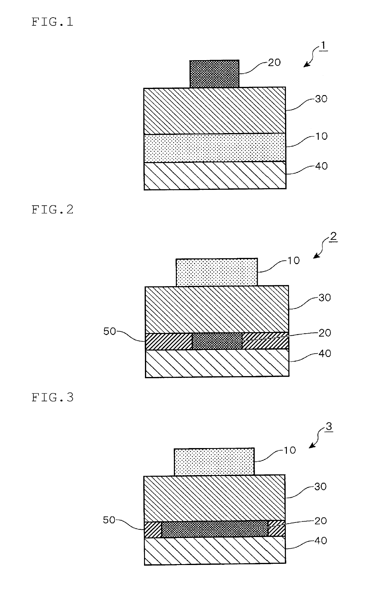
[0189]An n-type Si substrate having a resistivity of 0.001 Ω·cm (a diameter of 4 inches and a thickness of 250 μm) was disposed in a sputtering apparatus (E-2005 manufactured by Anelva Corporation), and the following laminated electrode was formed. Additionally, a substrate back surface was treated with 100 nm of Ti / 50 nm of Au to eliminate a contact resistance with a prober at measurement. Initially, a film of Ti was formed in a thickness of 15 nm with DC of 50 W in an Ar atmosphere, next a film of Pd was formed in a thickness of 50 nm with DC of 50 W in the Ar atmosphere, and finally, as a Schottky electrode, a film of PdO was formed in a thickness of 20 nm with DC of 50 W in a mixed gas atmosphere of Ar and O2.

[0190]Next, this substrate was set together with an areamask for a semiconductor in a sputtering apparatus (CS-200 manufactured by ULVAC), and as a withstand voltage layer (a semiconductor layer), a film of InGaZnO was formed in a thickness of 200 nm (In:Ga:Zn (atom ratio)=...

examples 2 to 5 , 9 , 18 and 19

Examples 2 to 5, 9, 18 and 19

[0224]The procedure of Example 1 was repeated except that film forming conditions were changed as shown in Tables 2-1 and 2-2, to manufacture and evaluate semiconductor devices. Tables 2-1 and 2-2 show the results. Furthermore, the semiconductor devices of these examples satisfied the formula (I).

example 6

[0225]The procedure of Example 1 was repeated except that film forming conditions were changed as shown in Table 2-1, to manufacture and evaluate a semiconductor device. Table 2-1 shows the result. Additionally, the semiconductor device of this example satisfied the formula (I).

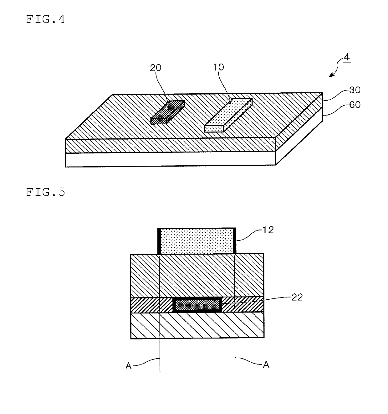
[0226]In this example, a material of the ohmic electrode of Example 1 was changed from Mo to Ti.

[0227]When the L was evaluated, contrast of a TEM image containing InGaZnO was shorter than 200 nm due to extraction of oxygen from the Ti electrode, and it was confirmed that a thickness of a semiconductor layer was 180 nm.


PUM


Abstract

A semiconductor device 1 which comprises a pair of an ohmic electrode 20 and a Schottky electrode 10 separated from each other, and a semiconductor layer 30 in contact with the ohmic electrode 20 and the Schottky electrode 10, and which satisfies the following formula (I):n<ɛ⁢⁢VeqL2(I)in which n is a carrier concentration (cm−3) of the semiconductor layer, ε is a dielectric constant (F / cm) of the semiconductor layer, Ve is a forward effective voltage (V) between the ohmic electrode and the Schottky electrode, q is an elementary charge (C), and L is a distance (cm) between the ohmic electrode and the Schottky electrode.

Description

TECHNICAL FIELD[0001]The invention relates to a semiconductor device, and a Schottky barrier diode, a junction transistor, an electronic circuit as well as an electric apparatus using the semiconductor device.BACKGROUND ART[0002]As power semiconductor materials to actualize large current and low power consumption, Si can first be enumerated, and new materials of SiC, GaN and others can also be enumerated. In addition, gallium oxide and diamond are also promising as next generation materials. On the other hand, they are basically used in the form of monocrystals, and therefore they have drawbacks that growth of the monocrystals on different substrates is difficult and selection of the substrates is limited.[0003]With respect to SiC, a preferable crystal structure as the power semiconductor is 4H—SiC, and as dielectric breakdown field of the same, 3 MV / cm or more is actualized. However, inconformity of lattices is large, and hence it is difficult to achieve epitaxial growth of the mon...

Claims


Application Information

Patent Timeline
Patent Type & Authority Patents(United States)
IPC IPC(8): H01L29/10H01L21/02H01L29/872H01L29/12H01L29/24H01L29/812H01L29/47H01L29/45
CPCH01L29/247H01L21/02381H01L21/02565H01L29/812H01L29/872H01L21/02631H01L29/47H01L29/45H01L29/24H01L29/517
Inventor TSURUMA, YUKISEKIYA, TAKASHITOMAI, SHIGEKAZUKAWASHIMA, EMIUEOKA, YOSHIHIRO
Owner IDEMITSU KOSAN CO LTD
Why Eureka
Try Eureka