
Display device and method for manufacturing the same

a technology of a display device and a manufacturing method, applied in the field of display devices, can solve the problem of becoming more difficult to constitute one pixel with such three sub-pixels, and achieve the effect of varying the luminescent color and

Active Publication Date: 2019-08-13
SONY CORP
View PDF19 Cites 0 Cited by
  • Summary
  • Abstract
  • Description
  • Claims
  • Application Information

AI Technical Summary

Benefits of technology

The present disclosure describes a method for manufacturing a display device with improved light shielding to prevent interference between neighboring light emitting elements. The method includes creating a light shielding layer inside the grooves where the light emitting elements are placed. This helps to reduce the amount of light that enters the display device and improves its overall performance. The method also involves using a self-alignment method to form the grooves and micronize the light emitting elements. Additionally, the patent text defines a relationship between the bottom of the groove and the top surface of the light reflecting layer to prevent contact between them, which can affect the performance of the display device. Overall, this patent provides technical improvements to the manufacturing process of display devices.

Problems solved by technology

However, it becomes more difficult to constitute one pixel with such three sub-pixels as the pixel pitch becomes finer.

Method used


Image

  • Display device and method for manufacturing the same
  • Display device and method for manufacturing the same
  • Display device and method for manufacturing the same

Examples


example 1

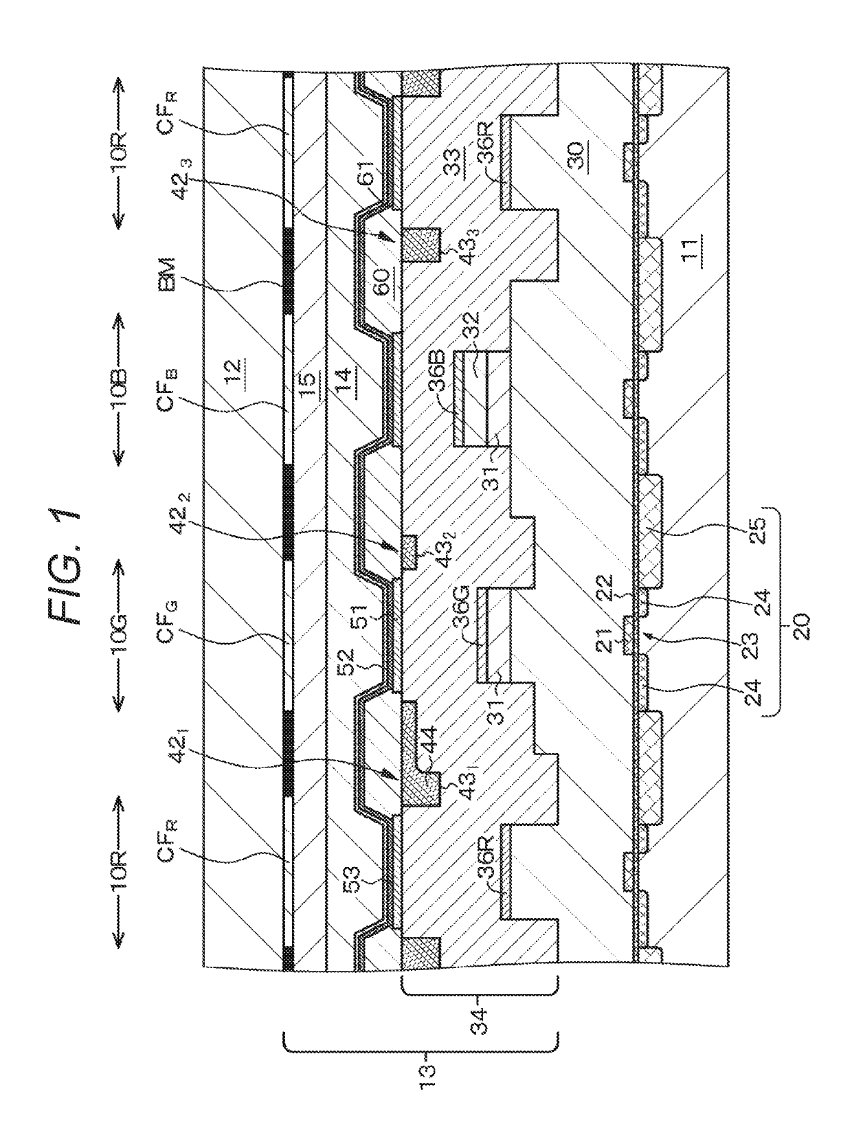
[0099]Example 1 relates to the display device of the present disclosure and a method for manufacturing the display device. FIG. 1 illustrates a schematic partial cross-sectional view of the display device of the present disclosure. The display device of Example 1 is specifically constituted by an organic EL display device. The light emitting element of Example 1 is specifically constituted by an organic EL element.

[0100]The display device of Example 1 or a display device in the method for manufacturing the display device of Example 1

[0101]includes a plurality of pixels each including a first light emitting element 10R, a second light emitting element 10G, and a third light emitting element 10B, arranged in a two-dimensional matrix.

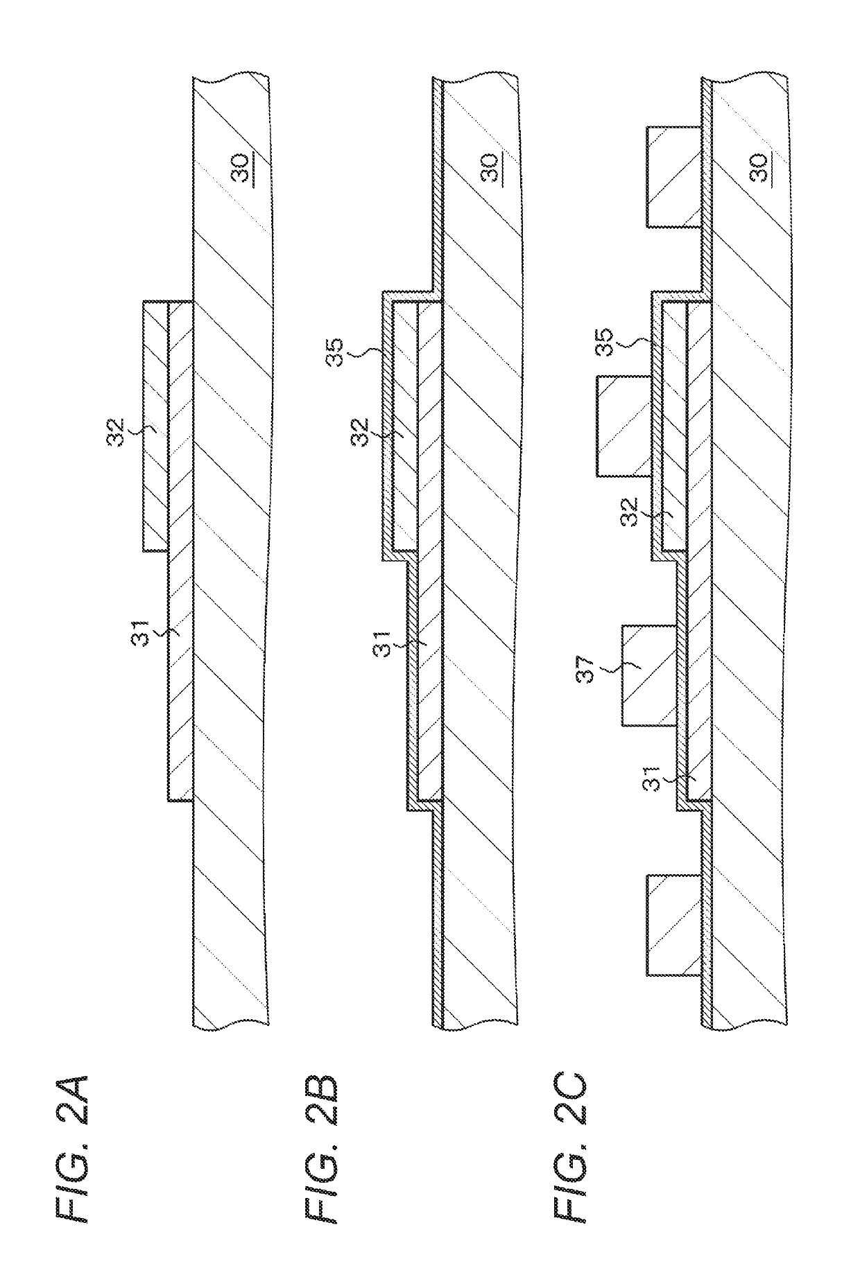
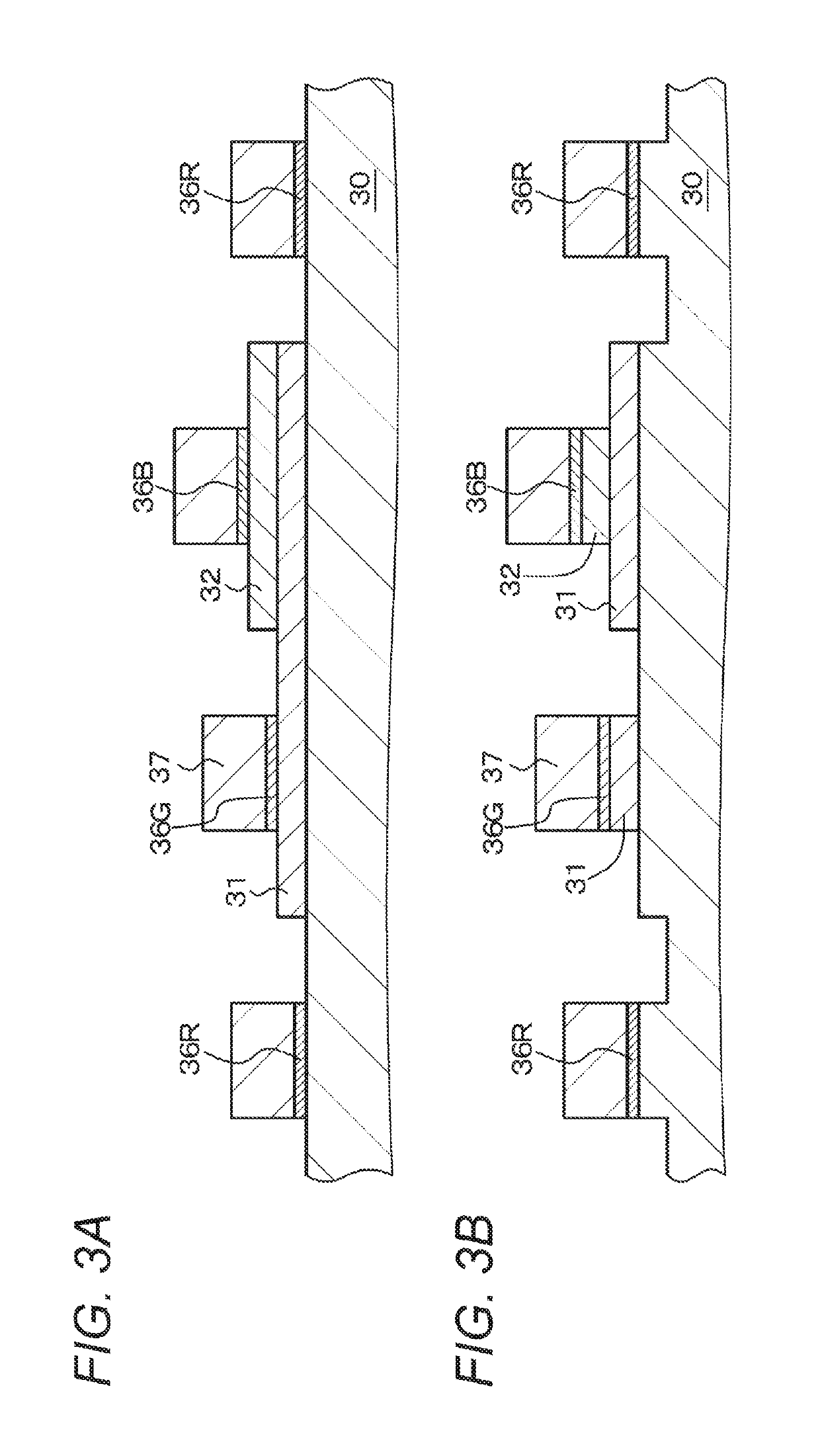
[0102]Each of the pixels includes a lowermost layer / interlayer insulation layer 30, a first interlayer insulation layer 31 formed on the lowermost layer / interlayer insulation layer 30, a second interlayer insulation layer 32 formed on the first interlayer ...

example 2

[0164]Example 2 is a modification of Example 1. As illustrated in a schematic partial cross-sectional view in FIG. 7, an insulation film 62 including SiON, SiO2, or a polyimide resin is formed on a region of the uppermost layer / interlayer insulation layer 33 where the first electrode 51 is not formed. The organic layer 53 is formed on the first electrode 51 and the insulation film 62 which are flat as a whole, and the organic layer 53 is also flat. In this way, by forming the organic layer 53 on the first electrode 51 and the insulation film 62 which are flat as a whole, it is possible to prevent occurrence of a problem such as abnormal light emission at an end of an opening of the insulation film.

[0165]In the display device of Example 2, for example, in a similar step to [Step-170] of Example 1, by performing a flattening treatment after the insulation film 62 is formed on the entire surface, for example, on the basis of a CVD method, it is only required to leave the insulation fil...

example 3

[0166]Example 3 is a modification of Example 1.

[0167]By the way, a phenomenon that a leakage current flows between the first electrode in a certain light emitting element and the second electrode constituting an adjacent light emitting element may occur. In addition, when such a phenomenon occurs, light emission occurs in a light emitting element which should not emit light originally. Meanwhile, intensity of an electric field in a light emitting element which should emit light is reduced. As a result, blurring may occur in an image, or the chromaticity of the entire pixels may be shifted from desired chromaticity. In order to solve such a problem, in Example 3, at the time of film formation of the organic layer 53, at least a part of a part (specifically, for example, hole injection layer) of the organic layer 53 is made discontinuous at an end of the insulation film 60, specifically, at an edge of the opening 61 disposed in the insulation film 60. In this way, for example, by maki...


PUM


Abstract

A display device includes a plurality of pixels each including a first light emitting element with a first light reflecting layer, a second light emitting element with a second light reflecting layer, and a third light emitting element with a third light reflecting layer, arranged in a two-dimensional matrix. Each of the light emitting elements includes a first electrode, an organic layer, and a second electrode. Grooves that each have a light shielding layer are formed in a boundary region between the light emitting elements. A bottom of the first groove and a bottom of the third groove are located at a position higher than a top surface of the first light reflecting layer. A bottom of the second groove is located at a position higher than a top surface of the second light reflecting layer.

Description

TECHNICAL FIELD[0001]The present disclosure relates to a display device and a method for manufacturing the display device.BACKGROUND ART[0002]In recent years, as a display device substituted for a liquid crystal display device, an organic electroluminescence display device (hereinafter, also simply abbreviated as an “organic EL display device”) using an organic electroluminescence element (hereinafter, also simply abbreviated as an “organic EL element”) has attracted attention. The organic EL display device is a self-luminous type, has a characteristic of low power consumption, and is considered to have sufficient responsiveness even to a high-definition high-speed video signal. Development and commercialization of the organic EL display device for practical use are keenly proceeding.[0003]In the organic EL display device, high contrast and high color reproducibility can be realized, for example, by constituting one pixel with three sub-pixels (light emitting elements) constituted b...

Claims


Application Information

Patent Timeline
Patent Type & Authority Patents(United States)
IPC IPC(8): H01L27/32H01L51/56H05B33/14H01L51/52G09F9/30H05B33/24
CPCH01L27/3246G09F9/30H01L27/32H01L27/3211H05B33/24H01L51/5271H01L51/56H05B33/145H01L27/3272H05B33/12H05B33/22H05B33/10H10K59/35H10K59/38H10K59/124H10K59/126H10K59/122H10K59/1201H10K59/876H10K59/8792H10K59/878H10K59/1213H10K50/852H10K50/856H10K59/00H10K71/00H10K50/865H10K59/12
Inventor OHCHI, TOMOKAZU
Owner SONY CORP
Learn More