Supercharge Your Innovation With Domain-Expert AI Agents!

Liquid crystal panel and array substrate thereof

a technology of array substrates and liquid crystal panels, which is applied in the direction of electrical appliances, semiconductor devices, instruments, etc., can solve the problems of serious affecting the optical grade of the picture, and achieve the effects of low distortion degree, high optical grade, and reduced brightness of white sub-pixels

Active Publication Date: 2019-08-27
WUHAN CHINA STAR OPTOELECTRONICS TECH CO LTD
View PDF14 Cites 0 Cited by
  • Summary
  • Abstract
  • Description
  • Claims
  • Application Information

AI Technical Summary

Benefits of technology

The patent text describes a new design for a pixel structure in a liquid crystal display that reduces distortion and improves optical quality. The design includes three primary color sub-pixels and one white sub-pixel, with the switching elements in the white region being arranged in a way that reduces brightness. This results in a brighter display from the three primary colors and reduces distortion in the overall display. The technical effect is a more visually appealing and high-quality liquid crystal display.

Problems solved by technology

Therefore, as compared with the RGB liquid crystal panel, when a single color picture or a multiple color picture is displayed on the RGBW liquid crystal panel, the RGBW liquid crystal panel 1a has lower brightness during single color picture display and picture distortion will be resulted in, which will seriously affect the optical grade of the picture.

Method used


Image

  • Liquid crystal panel and array substrate thereof
  • Liquid crystal panel and array substrate thereof
  • Liquid crystal panel and array substrate thereof

Examples


Embodiment Construction

[0026]The present disclosure will be further explained hereinafter combining the accompanying drawings.

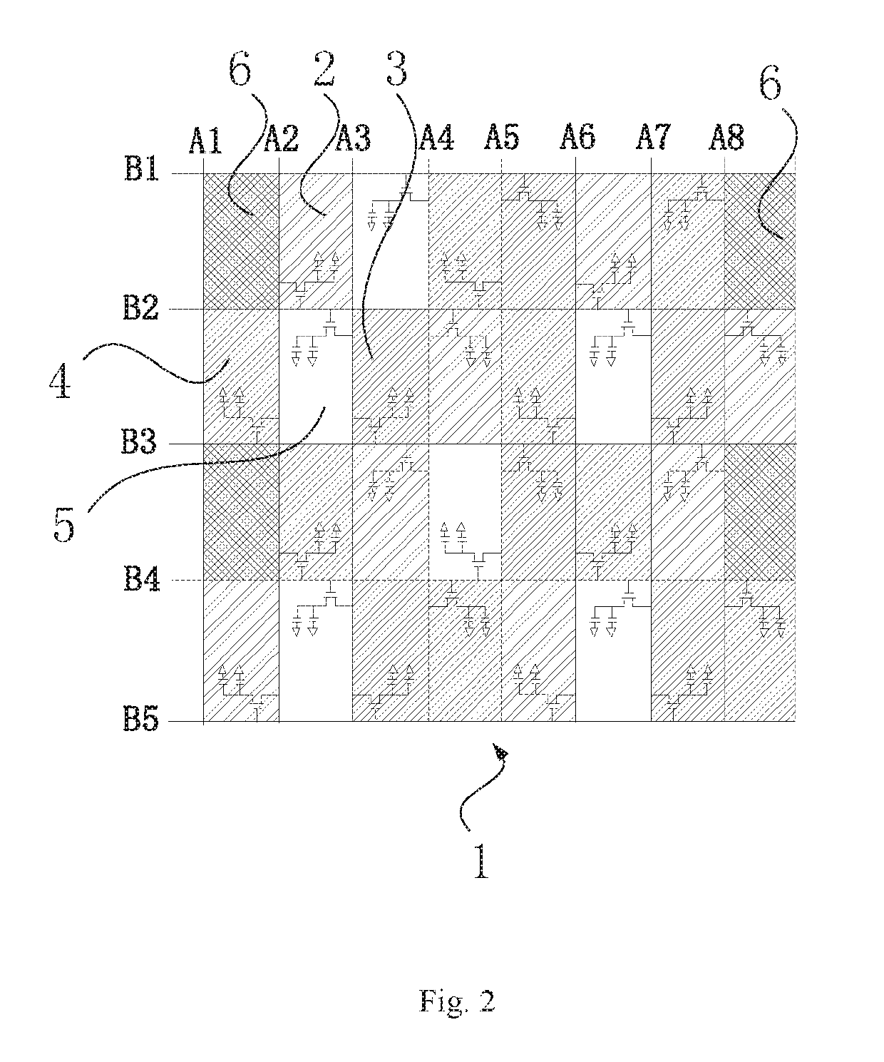
[0027]FIG. 2 schematically shows a liquid crystal panel 1 in a first embodiment of the present disclosure. The liquid crystal panel 1 comprises an array substrate, a color filter substrate and a liquid crystal layer. The array substrate and the color filter substrate are arranged in parallel with each other, and liquid crystals are filled between the array substrate and the color filter substrate to form the liquid crystal layer.

[0028]The color filter substrate comprises an upper polarizer, a glass baseplate, a color filter, a common electrode layer and an upper alignment film. The upper polarizer, the glass baseplate, the color filter, the common electrode layer and the upper alignment film are laminated together.

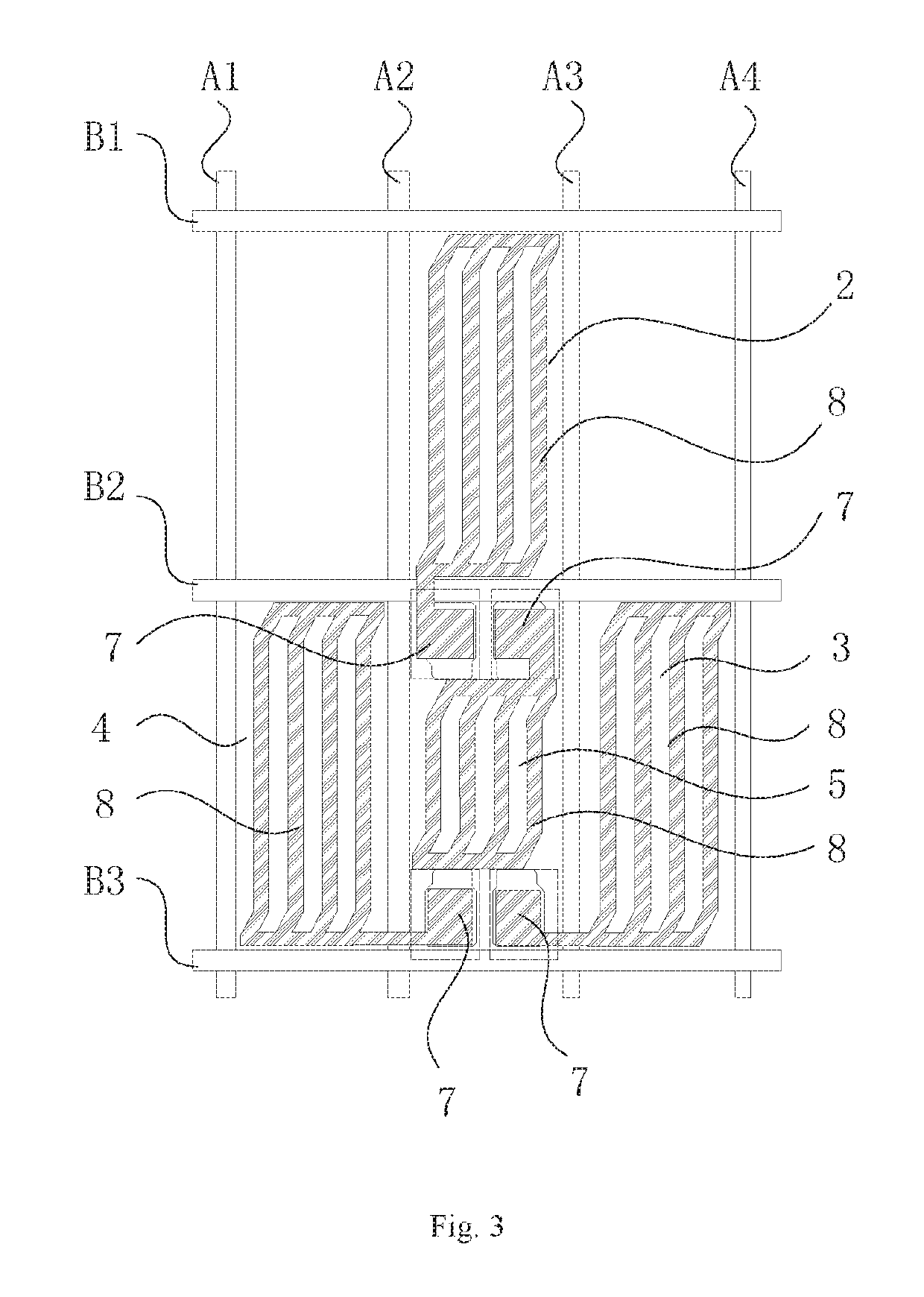
[0029]The array substrate comprises a lower alignment film, a TFT array layer, a transparent baseplate and a lower polarizer. The lower alignment film, the TFT array laye...


PUM

PropertyMeasurementUnit
transparentaaaaaaaaaa
colorsaaaaaaaaaa
brightnessaaaaaaaaaa

Abstract

Disclosed is an array substrate, which includes: a transparent baseplate, wherein the transparent baseplate includes pixel regions on one surface thereof, and the pixel regions each include a white sub-pixel region, a first primary color sub-pixel region, a second primary color sub-pixel region and a third primary color sub-pixel region; a plurality of pixel electrodes that are arranged in the white sub-pixel region, the first primary color sub-pixel region, the second primary color sub-pixel region and the third primary color sub-pixel region respectively; and a plurality of switching elements that are arranged in one-to-one correspondence with the pixel electrodes and configured to switch the corresponding pixel electrodes, wherein the white sub-pixel region is provided with a plurality of switching elements. A colored picture displayed by a liquid crystal display screen using this array substrate or liquid crystal panel can have a low distortion degree and a high optical grade.

Description

CROSS-REFERENCE TO RELATED APPLICATIONS[0001]The present application claims the priority of Chinese patent application CN 201610958139.6, entitled “Liquid crystal panel and array substrate thereof” and filed on Nov. 2, 2016, the entirety of which is incorporated herein by reference.FIELD OF THE INVENTION[0002]The present disclosure relates to liquid crystal display technology, and in particular, to a liquid crystal panel and an array substrate thereof.BACKGROUND OF THE INVENTION[0003]Currently, a liquid crystal display device generally comprises a backlight module and a liquid crystal panel. The liquid crystal panel covers the backlight module. The backlight module is used as a light source of the liquid crystal panel. The liquid crystal panel can modulate light emitted by the backlight module, so that images and colors can be displayed thereon. With development of liquid crystal display technology, it is required to increase brightness of a display screen as much as possible with p...

Claims


Application Information

Patent Timeline
Patent Type & Authority Patents(United States)
IPC IPC(8): H01L27/14G02F1/1368G02F1/1362G02F1/1343G02F1/1335G02F1/136
CPCG02F1/13624G02F1/133514G02F1/136286G02F1/1368G02F2201/40G02F2201/52G02F1/13606G02F1/134336G02F1/136209G02F2201/122G02F2201/123G02F1/134345
Inventor WANG, CONGLIAO, ZUOMIN
Owner WUHAN CHINA STAR OPTOELECTRONICS TECH CO LTD
Features
  • R&D
  • Intellectual Property
  • Life Sciences
  • Materials
  • Tech Scout
  • Unparalleled Data Quality
  • Higher Quality Content
  • 60% Fewer Hallucinations
Learn More