
Reducing back reflection in a photodiode

Active Publication Date: 2019-09-10
NOKIA SOLUTIONS & NETWORKS OY
View PDF1 Cites 0 Cited by
  • Summary
  • Abstract
  • Description
  • Claims
  • Application Information

AI Technical Summary

Benefits of technology

This patent describes a device that can change the way light passes through a waveguide. This is achieved by using a light absorber material that is angled in a way that ensures a gradual change in the refractive index between the waveguide and the composite section, which is a combination of the waveguide and the absorber material. This technology can help to improve the performance and efficiency of optical devices.

Problems solved by technology

Back reflection of individual PIC components becomes a large bottleneck for scaling PIC devices for higher performance applications.

Method used


Image

  • Reducing back reflection in a photodiode
  • Reducing back reflection in a photodiode
  • Reducing back reflection in a photodiode

Examples


Embodiment Construction

[0031]While the present teachings are described in conjunction with various embodiments and examples, it is not intended that the present teachings be limited to such embodiments. On the contrary, the present teachings encompass various alternatives and equivalents, as will be appreciated by those of skill in the art.

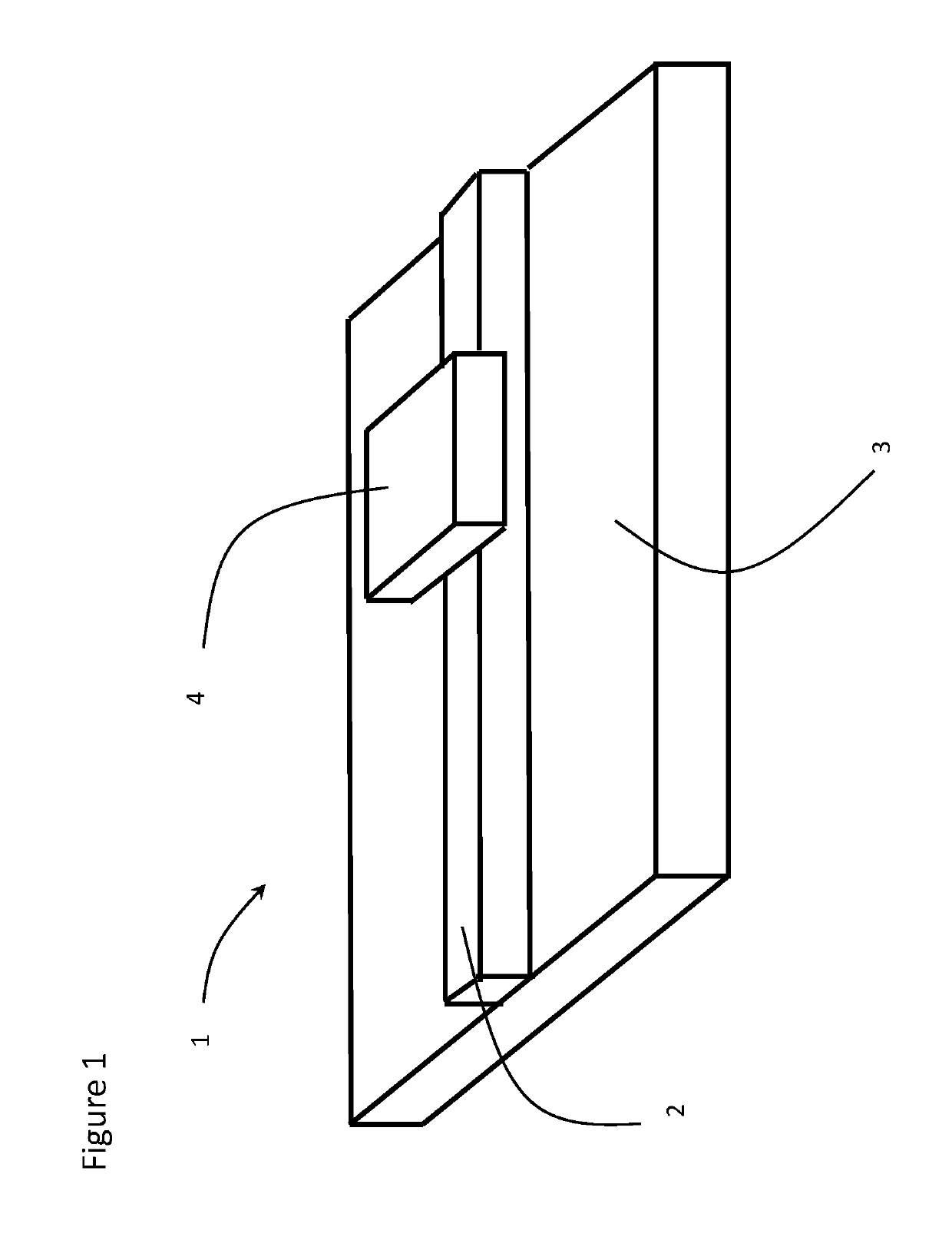
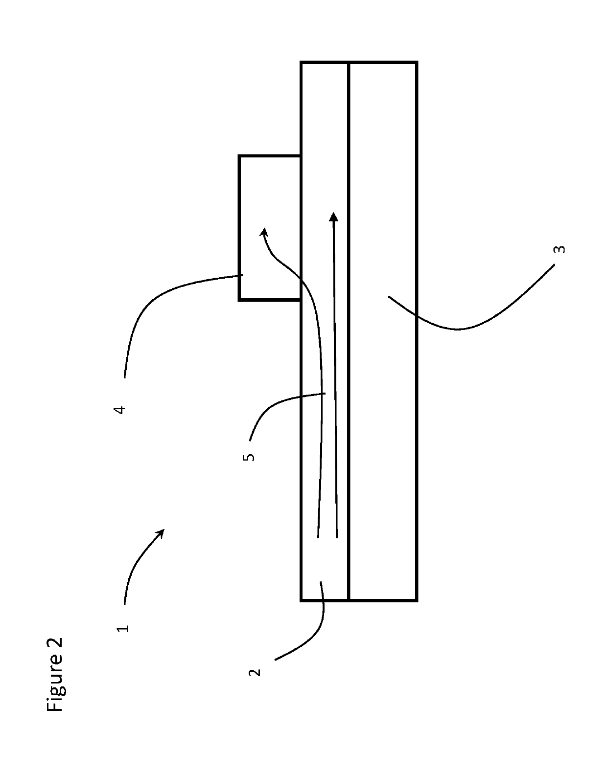
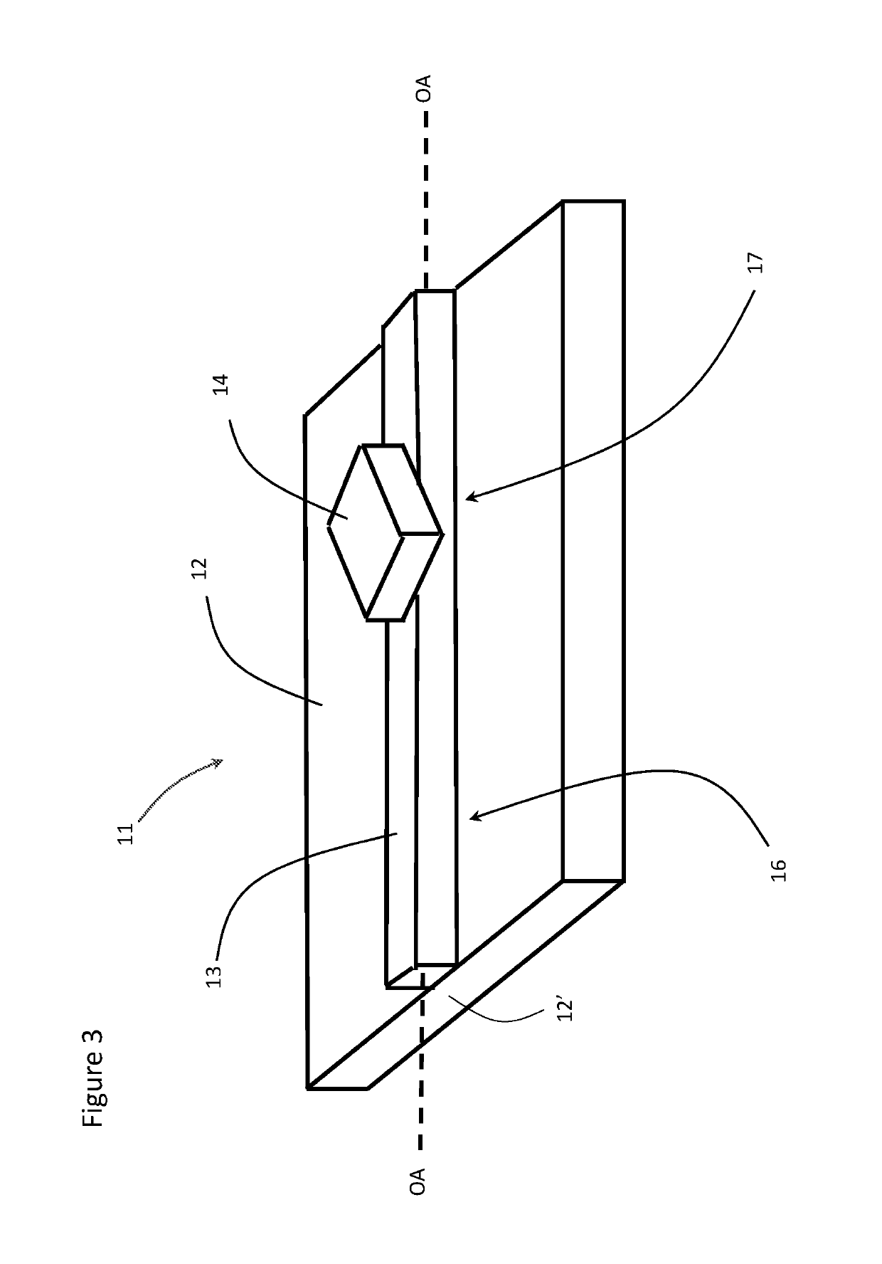
[0032]With reference to FIGS. 3 and 4, a photodetector, e.g. photodiode 11, of an exemplary embodiment of the present invention includes a substrate 12, on which is provided a waveguide 13, e.g. silicon, for transmitting an optical signal, typically a single mode optical signal. A cladding material, e.g. SiO2, (not shown) is typically provided surrounding the waveguide 13, with a lower index of refraction than the waveguide material, to contain the optical signal within the waveguide 13. A slab of light absorbing material 14, e.g. germanium, is provided adjacent to the waveguide 13 enabling the optical signal travelling in the waveguide 13 to be absorbed therein. Severa...


PUM


Abstract

The back reflection in photodiodes is caused by an abrupt index contrast between the input waveguide and the composite waveguide / light absorbing material. In order to improve the back reflection, it is proposed to introduce an angle between the waveguide and the leading edge of the light absorbing material. The angle will result in gradually changing the effective index between the index of the waveguide and the index of the composite section, and consequently lower the amount of light reflecting back.

Description

TECHNICAL FIELD[0001]The present invention relates to reducing back reflection in photodetectors, and in particular to reducing back reflection in a semiconductor photo-diode.BACKGROUND[0002]The demand for increased speeds and reduced costs in communication systems keeps growing, due in large part to the increase in mobile device usage, streaming media services, cloud computing, and big data analysis. Semiconductor waveguide, e.g. silicon, photonics has become the most promising technology to provide high-speed, low energy consumption and low cost next-generation data communication systems.[0003]Active devices, including photodetectors (PD), are a critical part of photonics integrated circuits (PIC), particularly for semiconductor waveguide, e.g. silicon, photonics (SiPh). A photodetector with high responsivity will compensate the channel insertion loss, and help fulfill the required link power budget. Several semiconductor absorbing materials, e.g. indium gallium arsenide (InGaAs),...

Claims


Application Information

Patent Timeline
Patent Type & Authority Patents(United States)
IPC IPC(8): H01L31/18G02B6/32H01L31/0232G02B6/12
CPCG02B6/327G02B6/12H01L31/18H01L31/02327G02B2006/12176G02B2006/12126G02B2006/12123G02B6/12004G02B2006/12061G02B6/4207
Inventor FATHOLOLOUMI, SAEEDLIU, YANGCHEN, YAOJIA
Owner NOKIA SOLUTIONS & NETWORKS OY
Learn More