Photodiode device monolithically integrating waveguide element with photodiode element type of optical waveguide
a technology of optical waveguide and photodiode element, which is applied in the direction of optical waveguide light guide, optical element, instrument, etc., can solve the problems of complex modulation, large temperature dependence of pd commercially available in the field, and high cost. , to achieve the effect of avoiding time constant, high speed operation and high speed operation
- Summary
- Abstract
- Description
- Claims
- Application Information
AI Technical Summary
Benefits of technology
Problems solved by technology
Method used
Image
Examples
first modification
[0059
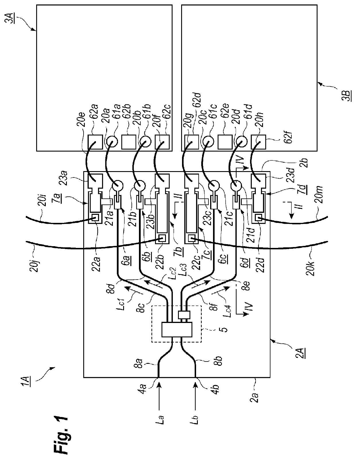
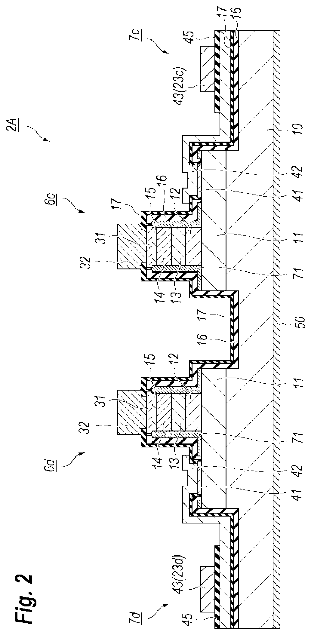
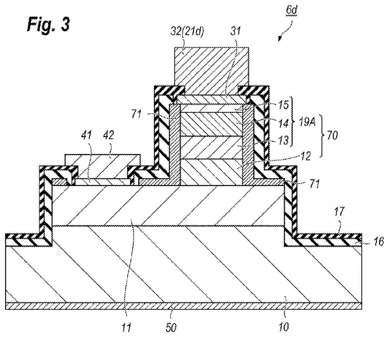
[0060]FIG. 12 is a cross sectional view of another PD device 2B that includes another PD element 6d and another waveguide element 8f, where FIG. 12 is taken along the line IV-IV indicated in FIG. 4. Both elements, 6d and 8f, are modified from the PD element 6d and the waveguide element 8f shown in FIG. 4. The arrangement of the PD device 2B shown in FIG. 12 has a feature that the PD device 2B omits the buffer layer 12 common to the PD element 6d and the waveguide element 8f but further provides an intermediate layer 18 in the PD element 6d. Other arrangements are substantially same with those shown in FIG. 4.
[0061]The PD element 6d includes, on the substrate 10, the conducting layer 11 and the PD structure 19B formed on the conducting layer 11 in the region D. The PD structure 19B provides stacked layers of, from the side of the conducting layer 11, the intermediate layer 18, the absorption layer 13, the p-type cladding layer 14, and the contact layer 15. The arrangements of th...
second modification
[0074
[0075]FIG. 13 is a cross sectional view of another PD device 2C also modified from that shown in FIG. 4, where the cross section shown in FIG. 13 is taken along the line IV-IV indicated in FIG. 1. The PD device 2C has a feature of further implementing the intermediate layer 18 without omitting the buffer layer 12. Other arrangements of the PD device 2C are substantially same with those, 2A and 2B, of the aforementioned embodiment.
[0076]In the arrangement of the PD device 2C shown in FIG. 13, a depletion layer at a reversed bias expands from the absorption layer 13 to the buffer layer 12 exceeding the intermediate layer 18, which may enable to further thin the absorption layer 13 without increasing the junction capacitance, or parasitic capacitance between the electrodes. A thinned absorption layer 13 may shorten the carrier transporting time within the absorption layer 13, which may enhance the response of the PD elements, 6a to 6d, in higher frequencies. The present modificati...
PUM
 Abstract
Description
Claims
Application Information


