Memory device and control method thereof
- Summary
- Abstract
- Description
- Claims
- Application Information
AI Technical Summary
Benefits of technology
Problems solved by technology
Method used
Image

Examples
Embodiment Construction
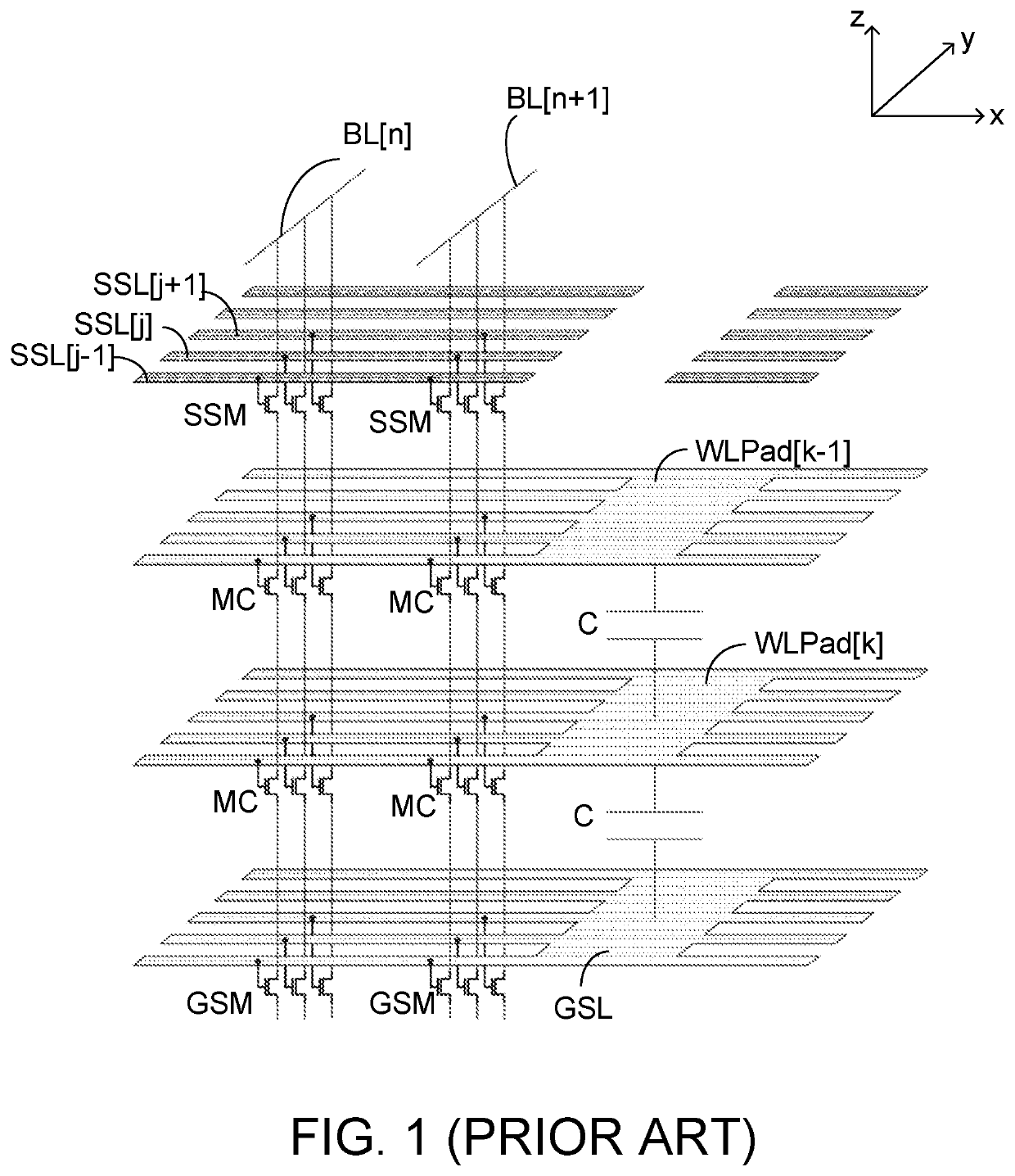
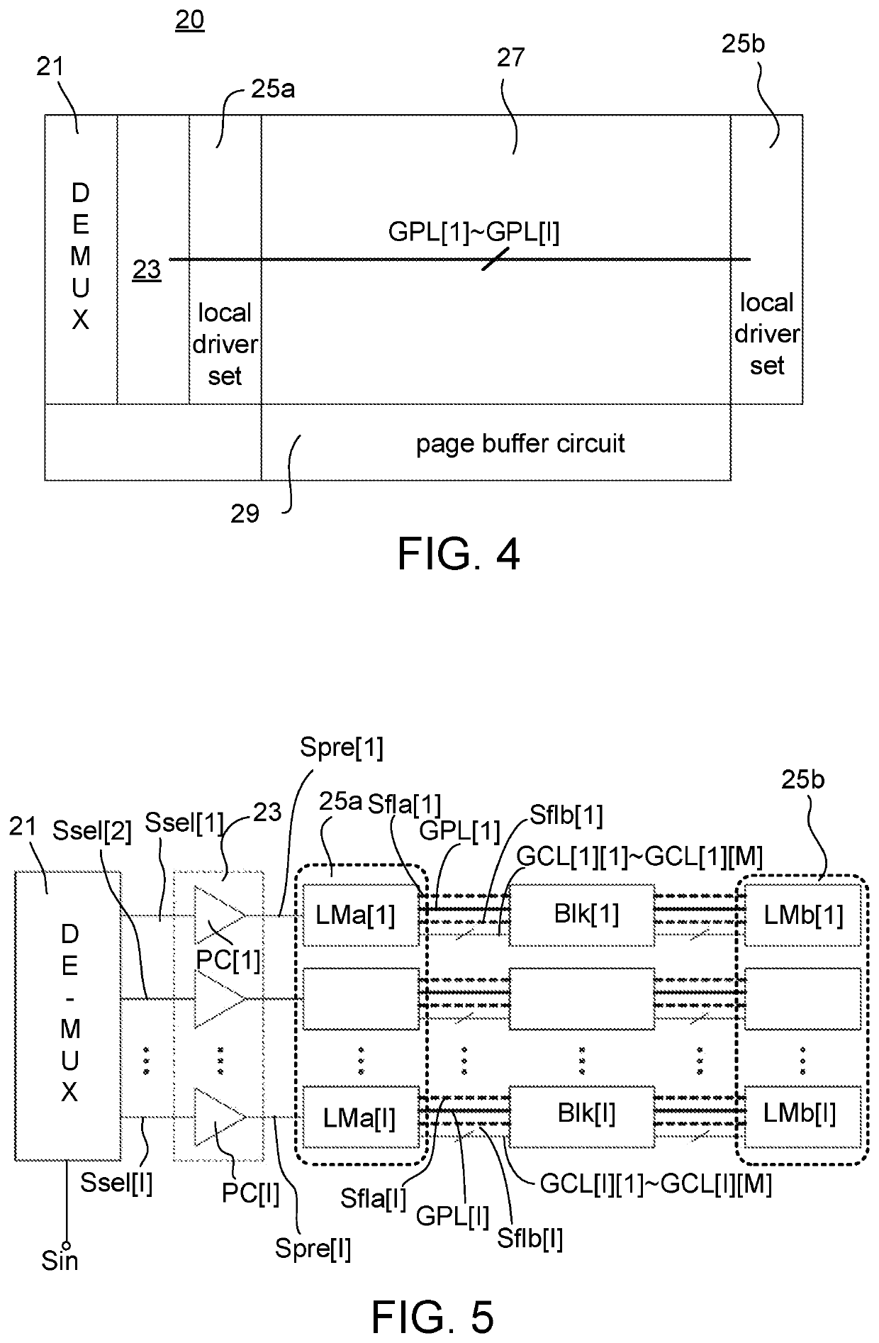
[0034]Please refer to FIG. 4 which is a schematic diagram illustrating a memory device according to an embodiment of the invention. The memory device 20 includes a demultiplexer circuit (DEMUX) 21, a pre-driver module 23, two local driver sets 25a and 25b, a page buffer circuit 29, I global power lines GPL[1]˜GPL[I] and a memory array 27. For illustration purposes, the memory array 27 in the embodiment includes memory blocks Blk[1]˜Blk[I], each of which includes one or more memory pages. The memory blocks Blk[1]˜Blk[I] correspond to the global power lines GPL[1]˜GPL[I], respectively. For example, the memory block Blk[i] corresponds to the global power line GPL[i].
[0035]The demultiplexer circuit 21 is electrically connected to the pre-driver module 23, and the pre-driver module 23 is electrically connected to the local driver set 25a and the local driver set 25b through the I global power lines GPL. The page buffer circuit 29 is electrically connected to the memory array 27. In view ...
PUM
 Abstract
Description
Claims
Application Information
 - Generate Ideas
- Intellectual Property
- Life Sciences
- Materials
- Tech Scout
- Unparalleled Data Quality
- Higher Quality Content
- 60% Fewer Hallucinations
Browse by: Latest US Patents, China's latest patents, Technical Efficacy Thesaurus, Application Domain, Technology Topic, Popular Technical Reports.
© 2025 PatSnap. All rights reserved.Legal|Privacy policy|Modern Slavery Act Transparency Statement|Sitemap|About US| Contact US: help@patsnap.com