Antenna device and electronic device

a technology of electronic devices and antennas, applied in the direction of instruments, radiating elements, and structural forms of radiating elements, can solve the problems of not revealing a connection structure, affecting the operation of the instrument, so as to reduce the inductance of the wiring conductor, prevent unnecessary magnetic coupling between the coil antenna and the wiring conductor, and reduce the effect of unnecessary magnetic coupling

Active Publication Date: 2020-04-21
MURATA MFG CO LTD
View PDF18 Cites 0 Cited by
  • Summary
  • Abstract
  • Description
  • Claims
  • Application Information

AI Technical Summary

Benefits of technology

[0011]Preferred embodiments of the present invention provide antenna devices that reduce or prevent interaction between a wiring conductor and a coil antenna provided on a board, such as a printed wiring board, and that have stable characteristics, and electronic devices including such antenna devices.
[0013]With this configuration, unnecessary magnetic coupling between the coil antenna and the wiring conductor is prevented. In addition, the inductance of the wiring conductor is reduced.
[0014]A distance between the first wiring conductor parallel extending portion and the second wiring conductor parallel extending portion is preferably smaller than a distance between the two connection portions. Accordingly, unnecessary magnetic coupling between the coil antenna and the wiring conductor is more effectively reduced or prevented.
[0015]The first wiring conductor parallel extending portion and the second wiring conductor parallel extending portion may be provided on layers (including surface layers) of the substrate that are different from each other. Accordingly, it is possible to make the interval between the first wiring conductor portion and the second wiring conductor portion smaller, so that the effect of reducing or preventing unnecessary magnetic coupling between the coil antenna and the wiring conductor and the effect of reducing the inductance of the wiring conductor are improved.
[0016]Preferably, the coil antenna has a winding axis parallel or substantially parallel to the principal surface of the substrate, and in a plan view of the substrate, the coil antenna overlaps the first wiring conductor parallel extending portion, and an end portion of the coil antenna is aligned or substantially aligned with an edge portion of the second wiring conductor parallel extending portion or overlaps the second wiring conductor parallel extending portion. Accordingly, a magnetic flux passing between the first wiring conductor portion and the second wiring conductor portion is reduced, so that the effect of reducing or preventing unnecessary magnetic coupling between the coil antenna and the wiring conductor is improved.
[0018]According to various preferred embodiments of the present invention, unnecessary magnetic coupling between the coil antenna and the wiring conductor is reduced or prevented, and the inductance of the wiring conductor is also reduced. Thus, interaction between the wiring conductor and the coil antenna provided on the board, such as a printed wiring board, is reduced or prevented, and an antenna device having stable characteristics and an electronic device including the antenna device are obtained.

Problems solved by technology

In Japanese Unexamined Patent Application Publication No. 2003-16409, the coil antenna is disposed within the case of the device, but Japanese Unexamined Patent Application Publication No. 2003-16409 does not disclose a connection structure with a wiring conductor provided on a printed wiring board.
However, as a result of research performed by the inventor of the present invention, it has been discovered that unnecessary coupling between the wiring conductor and the coil antenna becomes a problem or the wiring conductor has an effect on the characteristics of the antenna device.
For example, a problem has been discovered that due to unnecessary coupling between the wiring conductor and the coil antenna or the inductance of the wiring conductor, the characteristics of the coil antenna as a single component and the characteristics of the coil antenna in a state where the coil antenna is mounted on the board may differ greatly from each other.

Method used


Image

  • Antenna device and electronic device
  • Antenna device and electronic device
  • Antenna device and electronic device

Examples


first preferred embodiment

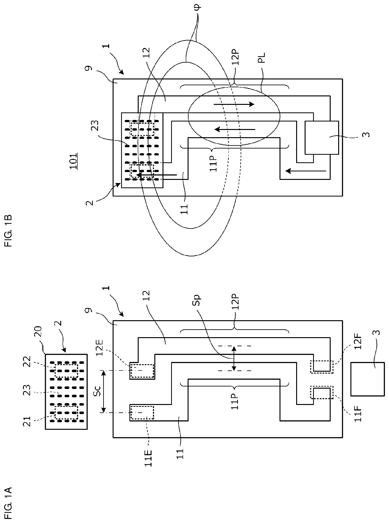
[0032]FIG. 1A is an exploded plan view of an antenna device according to a first preferred embodiment of the present invention, and FIG. 1B is a plan view of the antenna device 101 according to the first preferred embodiment of the present invention. The antenna device 101 includes a board 1, a coil antenna 2, and an RFIC 3. The board 1 includes an insulating substrate 9, and a first wiring conductor 11 and a second wiring conductor 12 that are provided on a principal surface (surface shown in FIGS. 1A and 1B) of the substrate 9.

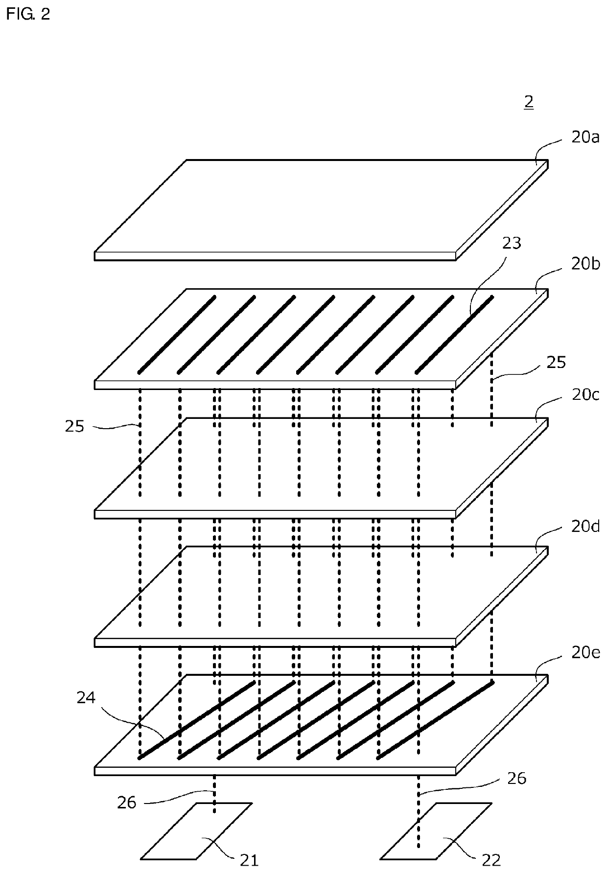
[0033]The coil antenna 2 includes a helically wound coil conductor 23 and two mounting electrodes 21 and 22 connected to the coil conductor 23.

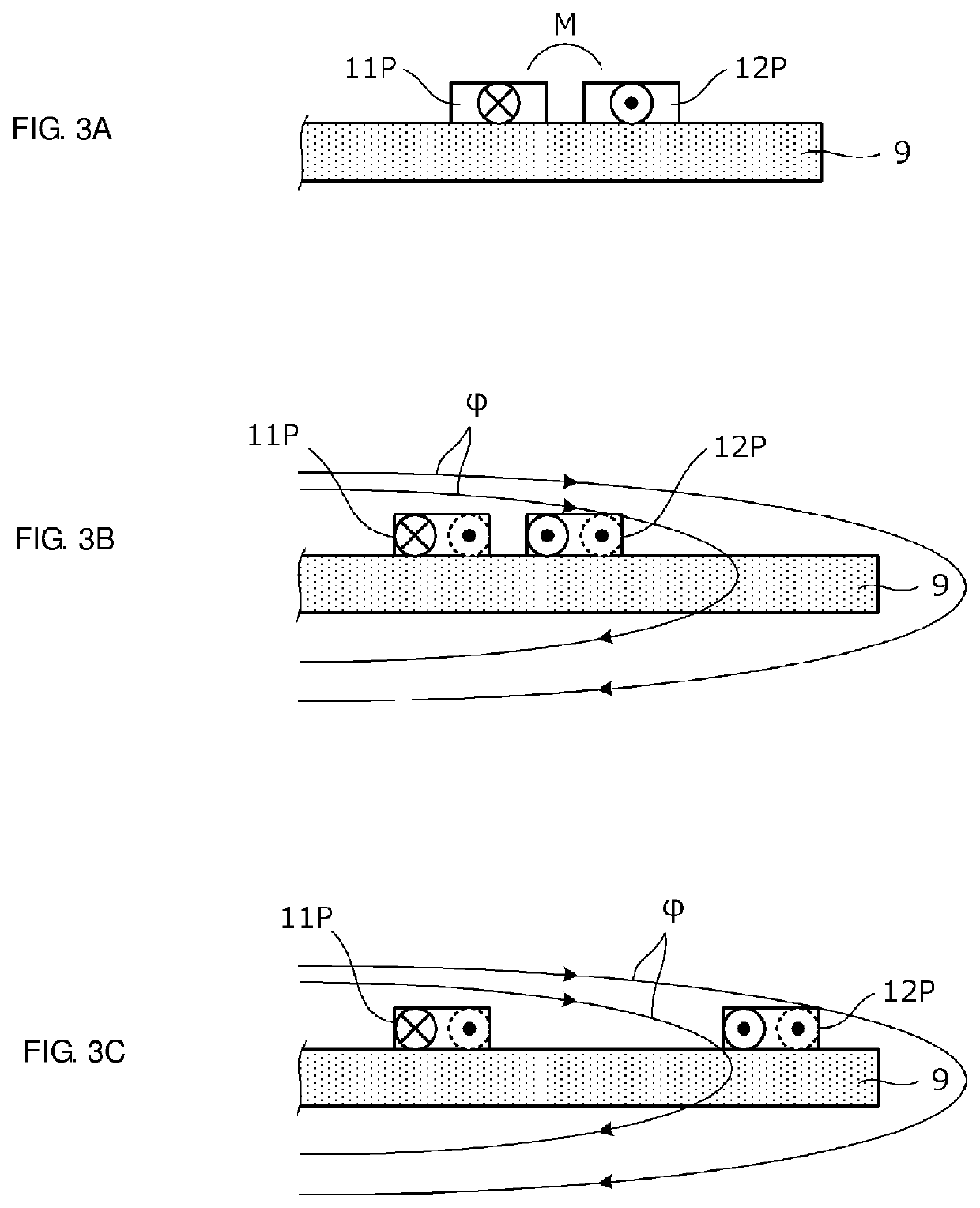
[0034]The first wiring conductor 11 includes a coil antenna connection portion 11E, an RFIC connection portion 11F, and a first wiring conductor parallel extending portion 11P. The second wiring conductor 12 includes a coil antenna connection portion 12E, an RFIC connection portion 12F, and a second wiring conductor p...

second preferred embodiment

[0048]FIG. 4A is a plan view of an antenna device 102 according to the second preferred embodiment of the present invention. FIG. 4B is an enlarged plan view of a parallel extending portion PL of the antenna device 102.

[0049]The antenna device 102 includes a board 1, coil antennas 2A and 2B, and an RFIC 3. The board 1 includes first wiring conductors 11A and 11B and a second wiring conductor 12.

[0050]Each of the coil antennas 2A and 2B includes a helically wound coil conductor and mounting electrodes. The coil antennas 2A and 2B are the same or substantially the same as the coil antenna 2 described in the first preferred embodiment. The coil antennas 2A and 2B each include a winding axis that is parallel or substantially parallel and adjacent to a principal surface of the substrate 9.

[0051]Unlike the antenna device 101 described in the first preferred embodiment, the antenna device 102 of the present preferred embodiment preferably includes the two coil antennas 2A and 2B, and the t...

third preferred embodiment

[0058]FIG. 6 is a perspective view of an antenna device 103A according to a third preferred embodiment of the present invention. FIG. 7A is a plan view of the antenna device 103A. FIGS. 7B and 7C are plan views of antenna devices 103B and 103C, which are modifications of the antenna device 103A. An RFIC is not shown in FIGS. 7A-7C.

[0059]The antenna device 103A includes a board 1, coil antennas 2A and 2B, and an RFIC. The board 1 includes first wiring conductors 11A, 11B, 11C, and 11D and a second wiring conductor 12. The first wiring conductors 11B, 11C, and 11D are provided on the upper surface of a substrate 9, and the first wiring conductor 11A and the second wiring conductor 12 are provided on the lower surface of the substrate 9. The first wiring conductor 11A and the first wiring conductor 11B are connected to each other by a via-conductor V1, and the first wiring conductor 11D and the second wiring conductor 12 are connected to each other by a via-conductor V2.

[0060]Each of t...


PUM


Abstract

An antenna device includes an insulating substrate, a coil antenna including a helically wound coil conductor and at least two mounting electrodes conducted to the coil conductor, and a wiring conductor disposed on the substrate and including connection portions connected to the mounting electrodes of the coil antenna. The wiring conductor includes a first wiring conductor parallel extending portion and a second wiring conductor parallel extending portion, and directions of currents flowing through the first wiring conductor parallel extending portion and the second wiring conductor parallel extending portion are opposite to each other with respect to a direction of a current flowing through the coil conductor.

Description

CROSS REFERENCE TO RELATED APPLICATIONS[0001]This application claims the benefit of priority to Japanese Patent Application No. 2015-018697 filed on Feb. 2, 2015 and is a Continuation Application of PCT Application No. PCT / JP2016 / 052867 filed on Feb. 1, 2016. The entire contents of each application are hereby incorporated herein by reference.BACKGROUND OF THE INVENTION[0002]1. Field of the Invention[0003]The present invention relates to an antenna device for use in a near field radio communication system, and an electronic device including the antenna device.[0004]2. Description of the Related Art[0005]In an RFID in the HF band, such as NFC (Near Field Communication), that is mounted on a mobile terminal, a coil antenna that magnetically couples with a communication counterpart-side antenna is used.[0006]For example, Japanese Unexamined Patent Application Publication No. 2003-16409 discloses a mobile device that includes an RFID tag and in which a coil antenna of the RFID tag is dis...

Claims


Application Information

Patent Timeline
Patent Type & Authority Patents(United States)
IPC IPC(8): H01Q1/52G06K7/10H01Q1/22H01Q21/00H01Q7/00H01Q1/36H04B5/00
CPCG06K7/10356H01Q1/2216H04B5/0037H01Q7/00H01Q1/362H04B5/0081H01Q21/00H01Q1/521
Inventor TENNO, NOBUYUKI
Owner MURATA MFG CO LTD
Why Eureka
Try Eureka