
Self-organized solid-state synthetic neuronal structure

a solid-state, self-organized technology, applied in the field of synthetic neurons, can solve the problems of limiting current and increasing voltage across the interface, and achieve the effect of changing the conductivity of the structur

Active Publication Date: 2020-05-26
INSTITUT NATIONAL DE LA RECHERCHE SCIENTIFIQUE
View PDF3 Cites 0 Cited by
  • Summary
  • Abstract
  • Description
  • Claims
  • Application Information

AI Technical Summary

Benefits of technology

This approach enables efficient and dynamic neural network operations with low activation energy, mimicking biological neurons, and supports fast electronic dynamics, facilitating the creation of deep neural networks with low power consumption and high complexity, overcoming the limitations of existing ANN technologies.

Problems solved by technology

The charge accumulation is increased by a flow of electric charges (a current), but eventually limits the current and increases the voltage across the interface.

Method used


Image

  • Self-organized solid-state synthetic neuronal structure
  • Self-organized solid-state synthetic neuronal structure
  • Self-organized solid-state synthetic neuronal structure

Examples


Embodiment Construction

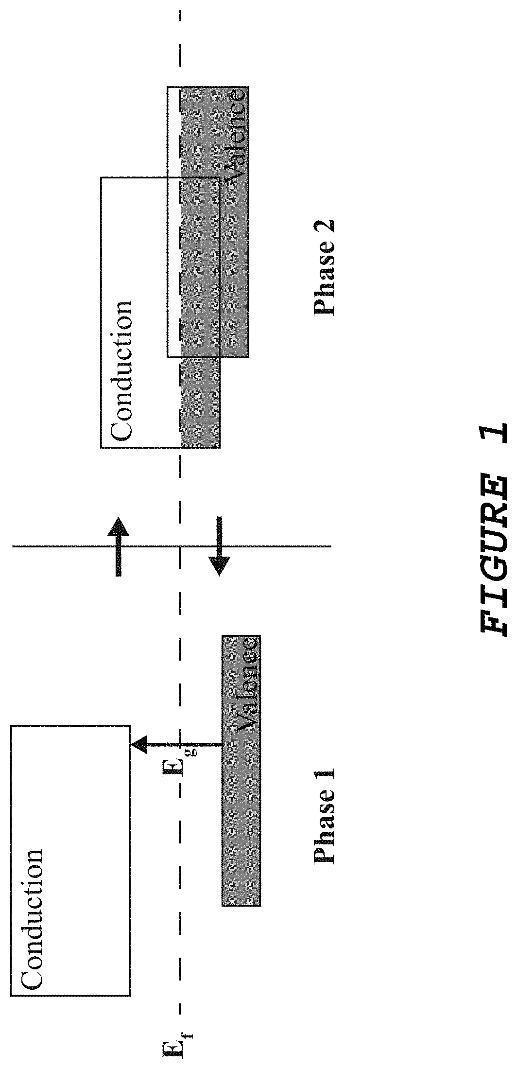
[0030]The present invention makes use of a low activation energy, semiconductor-metal phase transition (PT) material. In the exemplified embodiment of the invention, vanadium dioxide (VO2) is employed as such a PT material. VO2 is a semiconductor with a small energy bandgap at low temperatures which transitions into a metal upon activation. This activation can be induced by photoelectric effects, by direct electrical or potential bias or by temperature. The PT temperature of the material can be tuned and is typically around room temperature (300° K). When current densities are involved, typical values are around 1 nA / nm2 making it a low power and practical solution in micro-nanoelectronics. The response time of the material can range between femto-seconds for activation and picoseconds for relaxation, making it an excellent candidate for fast electronic dynamics.

[0031]In an exemplary embodiment of the invention, activation of the PT material is induced by a small electrical current ...


PUM


Abstract

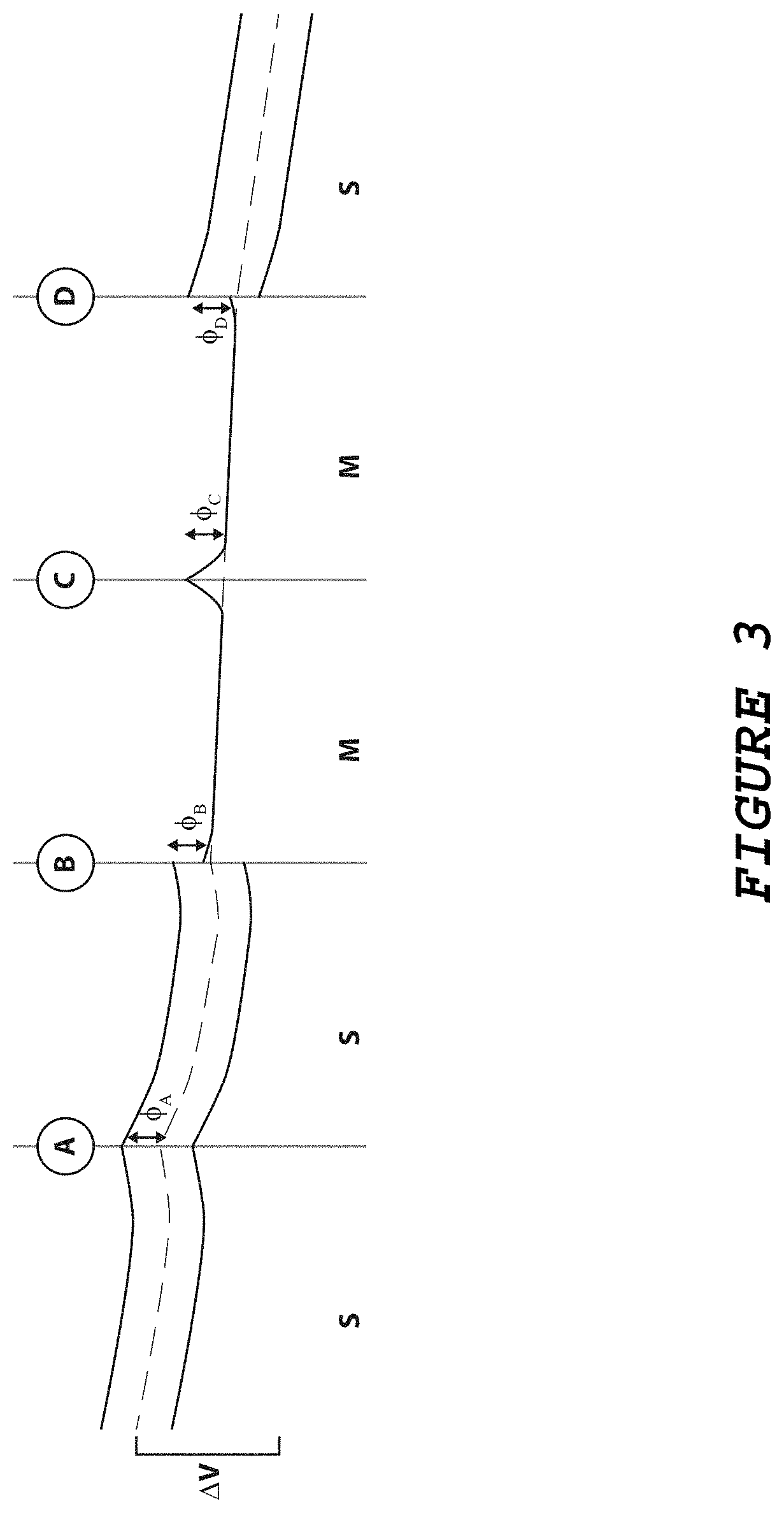
A synthetic neuronal structure makes use of a semiconductor-metal phase transition material having material regions separated by discontinuities. The discontinuities represent interfaces such that different phases in two adjacent regions result in a metal-semiconductor interface. The interface supports a charge accumulation and a discharge of accumulated charge when an activation energy provided, for example, by electrical current, localized heating or optical energy, reaches a threshold necessary for breakdown of a potential barrier presented by the interface, and thus mimics a leaky integrate-and-fire neuron. With many such interfaces distributed through the structure, the local inputs to a neuron become a weighted sum of energy from neighboring neurons. Thus, different combinations of signals at one or more inputs connected to the structure will favor different neural pathways through the structure, thereby resulting in a neural network.

Description

BACKGROUND OF THE INVENTION[0001]Field of the Invention[0002]This invention relates generally to the field of nanofabrication and, more specifically, to the construction of synthetic neurons.[0003]Description of the Related Art[0004]Artificial Neural Networks (ANN) are biology-inspired computer systems capable of addressing problems having a large number of unknown inputs. These systems are trained by repetition, with each iteration reinforcing specific neural pathways until an approximately suitable solution can be found. With the growth of computer-assisted decision making, ANN systems are increasingly at the heart of a wide variety of fields including search engines, voice recognition, vehicular / robotic automation and financial trading systems.[0005]The vast majority of existing ANN are software emulations. Commercial state of the art Graphics Processor Units (GPU) now allow for the implementation of deep neural networks for visual recognition. However, in the most powerful type ...

Claims


Application Information

Patent Timeline
Patent Type & Authority Patents(United States)
IPC IPC(8): G06N3/063G06N3/04
CPCG06N3/049G06N3/04G06N3/0635G06N3/065
Inventor LEPAGE, DOMINICCHAKER, MOHAMED
Owner INSTITUT NATIONAL DE LA RECHERCHE SCIENTIFIQUE
Learn More