Sensor package structure

a sensor and package technology, applied in the field of package structure, can solve the problems of air bubbles within the gap in the conventional sensor package structure, defects in the package structure, and difficult to completely fill, so as to achieve the effect of improving the problem associated

Active Publication Date: 2020-07-21
TONG HSING ELECTRONICS INDS
View PDF3 Cites 1 Cited by
  • Summary
  • Abstract
  • Description
  • Claims
  • Application Information

AI Technical Summary

Benefits of technology

[0005]In response to the above-referenced technical inadequacies, the present disclosure provides a sensor

Problems solved by technology

However, during the wire-bonding process implemented for the conventional sensor package structure, the periphery portion of the larger chip is suspended over the substrate, and hence a force exerted on the larger chip by the wire-bonding often induces defects in the package structure.
Mo

Method used


Image

  • Sensor package structure
  • Sensor package structure

Examples


first embodiment

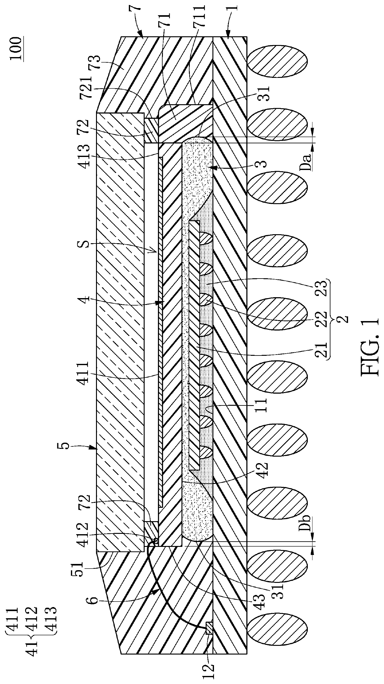
[0014]Please refer to FIG. 1, which illustrates the first embodiment of the disclosure. The first embodiment discloses a sensor package structure 100 that includes a substrate 1, an electronic chip 2 fixed on the substrate 1 by flip-chip bonding, a sealant 3 disposed on the substrate 1 and entirely embedding the electronic chip 2, a sensor chip 4 disposed on the sealant 3, a light-permeable sheet 5 corresponding in position to the sensor chip 4, a plurality of metal wires 6 electrically connecting the substrate 1 and the sensor chip 4, and a package body 7 disposed on the substrate 1.

[0015]It should be noted that FIG. 1 is presented as a cross-sectional view in order to clearly show the sensor package structure 100 of the embodiment. However, it should be realized that the portion of the sensor package structure 100 not shown in the drawing should have corresponding structures similar or identical to those in FIG. 1. For example, FIG. 1 only shows one of the metal wires 6, but the p...

second embodiment

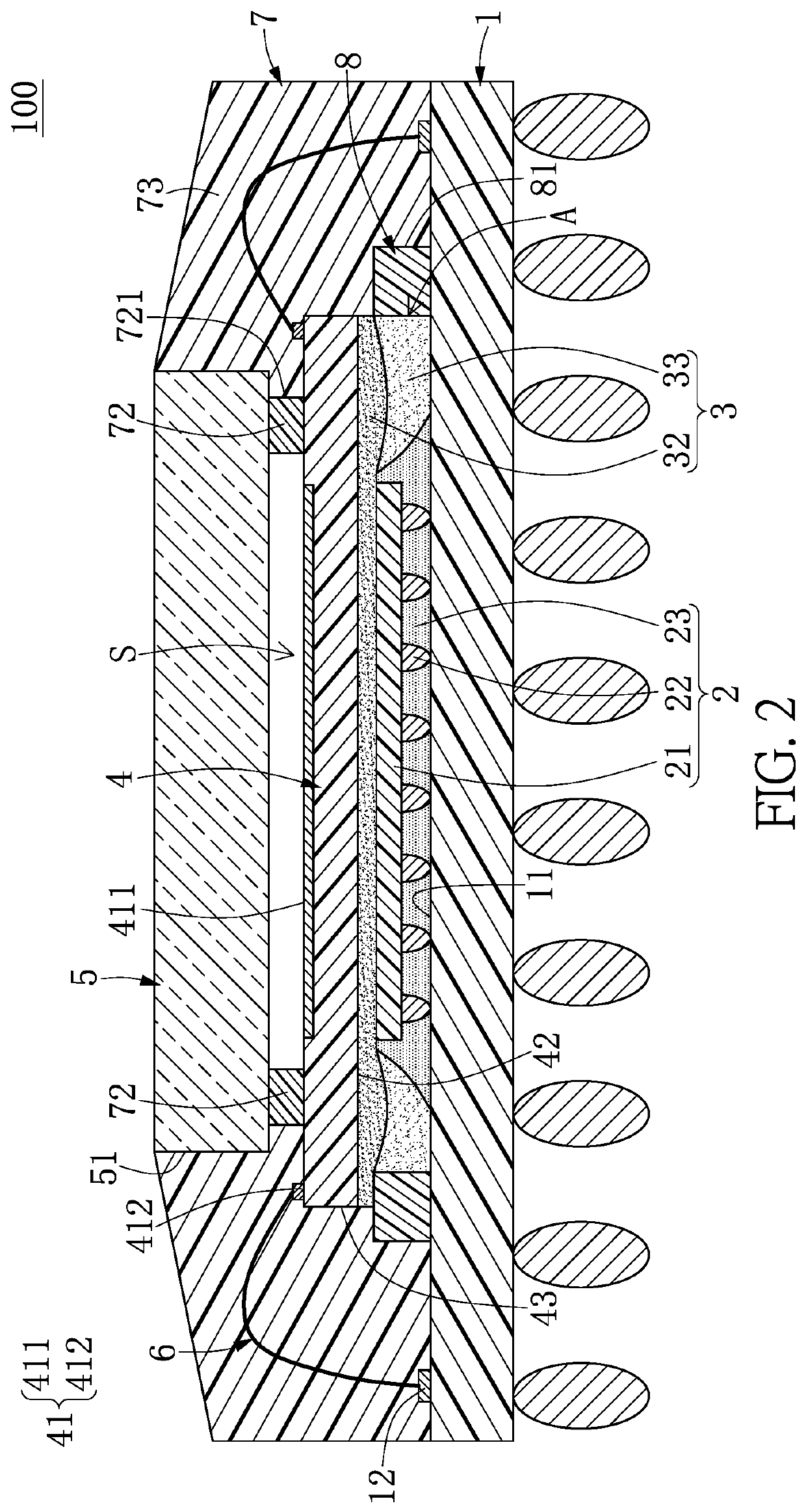
[0037]A reference is made to FIG. 2 which shows a second embodiment of the disclosure. The present embodiment is similar to the first embodiment, the common points between the embodiments shall not be recited again, and the main distinction of the embodiment differing from the first embodiment is described as follows. The sensor package structure 100 in this embodiment further includes a retaining wall 8, the sealant 3 includes a bottom layer 32 and an adhesive layer 33, and some components of the sensor package structure 100 are disposed in correspondence to the retaining wall 8.

[0038]Specifically, the retaining wall 8 in the embodiment is ring-shaped, and the retaining wall 8 is disposed on the substrate 1 to encompass an accommodating space A therein. The electronic chip 2 is arranged in the accommodating space A and mounted on the substrate 1 by flip-chip bonding. The bottom layer 32 is filled in the accommodating space A and surrounds an annular lateral side of the electronic c...


PUM


Abstract

A sensor package structure includes a substrate, an electronic chip fixed on the substrate by flip-chip bonding, a sealant disposed on the substrate and embedding the electronic chip therein, a sensor chip with a size larger than that of the electronic chip, a light-permeable sheet, a plurality of metal wires electrically connected to the substrate and the sensor chip, and a package body. A bottom surface of the sensor chip is disposed on the sealant to be spaced apart from the electronic chip. A lateral surface of the sensor chip is horizontally spaced apart from that of the sealant by a distance less than or equal to 3 mm. The package body is disposed on the substrate and covers the metal wires as well as the lateral sides of the sealant and the sensor chip. The light-permeable sheet is fixed above the sensor chip through the package body.

Description

CROSS-REFERENCE TO RELATED PATENT APPLICATION[0001]This application claims the benefit of priority to Taiwan Patent Application No. 107117000, filed on May 18, 2018. The entire content of the above identified application is incorporated herein by reference.[0002]Some references, which may include patents, patent applications and various publications, may be cited and discussed in the description of this disclosure. The citation and / or discussion of such references is provided merely to clarify the description of the present disclosure and is not an admission that any such reference is “prior art” to the disclosure described herein. All references cited and discussed in this specification are incorporated herein by reference in their entireties and to the same extent as if each reference was individually incorporated by reference.FIELD OF THE DISCLOSURE[0003]The present disclosure relates to a package structure, and more particularly to a sensor package structure.BACKGROUND OF THE DI...

Claims


Application Information

Patent Timeline
IPC IPC(8): H01L23/31H01L27/146
CPCH01L23/3114H01L23/3142H01L27/14625H01L27/14618H01L2224/83385H01L2924/16235H01L2224/16225H01L2224/73204H01L2224/32225H01L2224/32145H01L2224/73265H01L2924/15311H01L2924/16195H01L2924/00
Inventor CHEN, JIAN-RUYANG, JO-WEIHSIN, CHUNG-HSIENTU, HSIU-WEN
Owner TONG HSING ELECTRONICS INDS
Why Eureka
Try Eureka