Semiconductor light-emitting element and method for producing same

a technology of electromagnetic light and semiconductors, applied in the direction of semiconductor devices, basic electric elements, electrical appliances, etc., can solve the problems of deteriorating light extraction efficiency, total reflection of light, and inability to extract light incident at critical angles or greater to the outside, so as to prevent reflected light, improve light extraction efficiency, and suppress light loss

Active Publication Date: 2020-07-28
STANLEY ELECTRIC CO LTD
View PDF17 Cites 0 Cited by
  • Summary
  • Abstract
  • Description
  • Claims
  • Application Information

AI Technical Summary

Benefits of technology

[0011]However, when the inventors of the present invention examined the ultraviolet light-emitting element by the method described in Patent Literature 3 described above, it has been found that, even if the reflective layer is stacked on the semiconductor surface, sufficient light extraction efficiency may not be obtained depending on the layer configuration of the ultraviolet light-emitting element. Further, aluminum is used as a metal having a high reflectance with respect to ultraviolet light as the above-described reflective layer, but aluminum is extremely difficult to obtain an ohmic junction with respect to the p-type contact layer the p-type semiconductor layer, and so it has been found that there is a problem that the luminous efficiency is lowered.
[0013]in order to solve the above-described problems, the inventors of the present invention have conducted intensive studies. In an ultraviolet light-emitting element in which an n-type semiconductor layer, a light-emitting layer, and a p-type semiconductor layer are stacked in this order on a support substrate, a p-type contact layer is formed on the p-type semiconductor layer (p-type cladding layer) in order to easily realize an ohmic contact with the p-type electrode and to reduce the contact resistance with the p-type electrode. As the p-type contact layer, a p-type AlGaN layer or a p-type GaN layer having a smaller band gap and a smaller Al composition than those of the p-type cladding layer is used. However, the inventors have found that, since the p-type AlGaN layer and the p-type GaN layer having low Al compositions used in the contact layer absorb ultraviolet light, even if the reflective layer is provided on the surface of the semiconductor layer, the p-type contact layer absorbs light before the light reaches the reflective layer, so that sufficient light extraction efficiency is not obtained. Therefore, as a result of detailed studies on the layer configuration in the ultraviolet light-emitting element having the aforementioned configuration, it has been found that ultraviolet light emitted from the light-emitting layer is totally reflected at the interface between the re-type semiconductor layer and air. As a result of further studies on the layer configuration of the ultraviolet light-emitting element, it has been found that the light extraction efficiency from the light extraction surface of the support substrate is improved by controlling the exposed area of the n-type semiconductor layer and the exposed areas of the p-type contact layer and the p-type electrode in the semiconductor layer of the ultraviolet light-emitting element, whereby the present invention has been completed.
[0022]According to the present invention, is possible to improve the light extraction efficiency from the light extraction surface in the ultraviolet light emitting element.
[0023]The ultraviolet light-emitting element of the present invention is characterized in that the exposed areas of the p-type contact layer and the p-type electrode which absorb the ultraviolet light emitted from the light-emitting layer are controlled, and that the exposed area of the n-type semiconductor layer which has the property of totally reflecting the ultraviolet light at the air interface is increased. With such a configuration of the present invention, light reflected internally at the light extraction surface forming the indented structure can be reflected (totally reflected) at the interface between the n-type semiconductor layer and air, and extracted to the outside from the light extraction surface. In addition, it is possible to prevent the reflected light from being absorbed by the p-type contact layer and the p-type electrode. Further, it is unnecessary to use a metal as the reflective layer, and the contact property of the electrode is not impaired. Furthermore, when a material having a high refractive index is used for the n-type semiconductor layer, the critical angle of total reflection occurring at the interface with air can be reduced, and most of the light can be reflected toward the light extraction surface without loss. In addition, when an n-type semiconductor layer and a support substrate having high transmittance to ultraviolet light are used, loss of light intensity can be suppressed even if the optical path length is lengthened by reflecting light a plurality of times.

Problems solved by technology

In particular, when light travels from a medium having a large refractive index to a medium having a small refractive index, total reflection of light occurs, so that light incident at a critical angle or greater cannot be extracted to the outside.
As a result, the proportion of light totally reflected at the interface increases, resulting in a problem of deterioration of the light extraction efficiency.
Although the light extraction efficiency is improved by such a method, the light extraction efficiency varies greatly depending on the shape of the indented structure and the emission wavelength Therefore, it cannot be said that sufficiently improved light extraction efficiency is achieved, and further improvement of the light extraction efficiency has been demanded.
However, not all the light can be extracted to the outside because there is light that cannot be extracted to the outside due to the influence of scattering or Fresnel reflection at the interface of the support substrate.

Method used


Image

  • Semiconductor light-emitting element and method for producing same

Examples


example 1

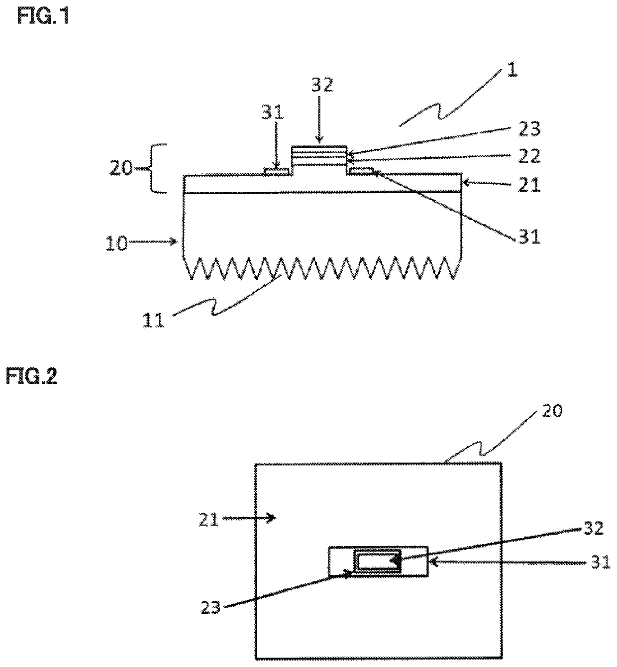
[0065]An n-type AlGaN layer, an active layer (light-emitting layer), and a p-type GaN were successively epitaxially grown on a single-crystal AlN substrate, which had been produced by an HVPE method, by an MOCVD method to obtain an ultraviolet light-emitting element wafer. The compositions were adjusted so that the emission wavelength was 265 nm.

[0066]An etching mask was formed on the wafer, and the region not covered with the etching mask was etched by an inductively coupled plasma (ICP) etching to partially expose the n-type semiconductor layer. Thereafter, an n-type electrode formed of Ti / Al / Au was formed on a part of the exposed portion of the n-type AlGaN layer, and then a p-type electrode formed of Ni / Au was sequentially formed on the p-type GaN layer. Then, a pad layer formed of Ti / Ni / Au was formed on the n-type electrode and the p-type electrode. Thereafter, the back surface of the AlN substrate was mechanically polished to obtain a wafer thickness of 100 μm.

[0067]In the pla...

examples 2 to 4

, Comparative Examples 1 to 4

[0072]An ultraviolet light-emitting element was produced and the optical output of the ultraviolet light-emitting element was measured with a photodiode in the same manner as that in Example 1 except that the electrodes were laid out under the conditions of Table 1 for the exposed area of the n-type semiconductor layer in the area of the ultraviolet light-emitting element, and the exposed areas of p-type contact layer and the p-type electrode. The results are shown in Table 1.

[0073]

TABLE 1Exposed areas of p-typecontact layer and p-typeOpticaln-typen-typep-typep-typeelectrode in theoutputAlGaN layerElectrodeElectrodeContact Layerremaining arearatioExample 187.1%6.7%5.4%0.8%48.1%2.13Example 280.4%13.4%5.4%0.8%31.6%2.07Example 373.8%20.1%5.4%0.8%23.7%2.06Example 466.2%27.7%5.4%0.8%18.3%2.02Comparative2.7%6.7%5.4%85.2%93.1%1.4Example 1Comparative2.9%13.4%5.4%78.3%86.2%1.45Example 2Comparative3.1%20.1%5.4%71.5%79.4%1.47Example 3Comparative3.2%27.7%5.4%63.7%71...


PUM

PropertyMeasurementUnit
refractive indexaaaaaaaaaa
absorption coefficientaaaaaaaaaa

Abstract

An ultraviolet light-emitting element includes a support substrate, a group III-V nitride semiconductor layer structure mounted on a mounting surface of the support substrate and including an n-type semiconductor layer, a light-emitting layer, a p-type cladding layer and a p-type contact layer stacked in this order on the support substrate, and an n-type electrode and a p-type electrode mounted on the n-type semiconductor and p-type contact layer, respectively. The support substrate has an indented portion formed on at least a part of a light emitting surface of the support substrate opposite to a mounting surface of the n-type semiconductor layer. An area of the n-type semiconductor layer surface exposed to the outside is at least 20% and at most 90% in largeness. Areas of the p-type contact layer surface and p-type electrode surface exposed to the outside are at least 5% and at most 50% in largeness.

Description

TECHNICAL FIELD[0001]The present invention relates to an ultraviolet light-emitting element such as a light-emitting diode (LED), and more particularly, to an ultraviolet light-emitting element which has an improved light extraction property of light emitted from the element to the outside.BACKGROUND ART[0002]In an ultraviolet light-emitting element, an n-type semiconductor layer, a light-emitting layer, and a p-type semiconductor layer are stacked in this order on a support substrate. Furthermore, a p-type electrode is formed on the p-type semiconductor layer, and an n-type electrode is formed on the n-type semiconductor layer. When a voltage is applied between the p-type electrode and the n-type electrode of the ultraviolet light-emitting element having such a configuration, holes of the p-type semiconductor layer and electrons of the n-type semiconductor layer recombine in the light-emitting layer, so as to radiate (emit) light corresponding to the band gap of the light-emitting ...

Claims


Application Information

Patent Timeline
Patent Type & Authority Patents(United States)
IPC IPC(8): H01L33/32H01L33/10H01L33/22H01L33/36
CPCH01L33/22H01L33/36H01L33/10H01L33/32
Inventor TAMARI, NAOKI
Owner STANLEY ELECTRIC CO LTD
Why Eureka
Try Eureka