Substrate for semiconductor light emitting elements, semiconductor light emitting element, method for producing substrate for semiconductor light emitting elements, and method for manufacturing semiconductor light emitting element

A technology of light-emitting elements and manufacturing methods, which is applied in semiconductor/solid-state device manufacturing, semiconductor devices, electrical components, etc., and can solve problems such as inability to obtain light emission efficiency

Active Publication Date: 2015-04-29
OJI HLDG CORP
View PDF14 Cites 4 Cited by
  • Summary
  • Abstract
  • Description
  • Claims
  • Application Information

AI Technical Summary

Problems solved by technology

In addition, it is described that the improvement effect of the light emission efficiency can hardly be obtained in the uneven structure with a pitch of 10...

Method used


Image

  • Substrate for semiconductor light emitting elements, semiconductor light emitting element, method for producing substrate for semiconductor light emitting elements, and method for manufacturing semiconductor light emitting element
  • Substrate for semiconductor light emitting elements, semiconductor light emitting element, method for producing substrate for semiconductor light emitting elements, and method for manufacturing semiconductor light emitting element
  • Substrate for semiconductor light emitting elements, semiconductor light emitting element, method for producing substrate for semiconductor light emitting elements, and method for manufacturing semiconductor light emitting element

Examples


no. 1 Embodiment approach

[0107]

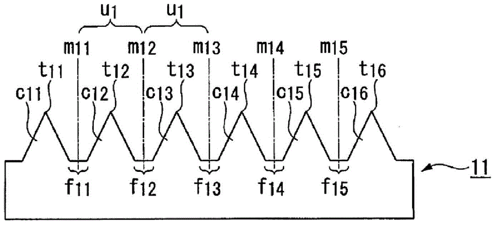
[0108] use figure 1 , 2 The substrate 11 for a semiconductor light emitting element according to one embodiment of the present invention will be described. Such as figure 1 As shown, the substrate 11 for a semiconductor light emitting element has a concavo-convex structure on one surface of the substrate.

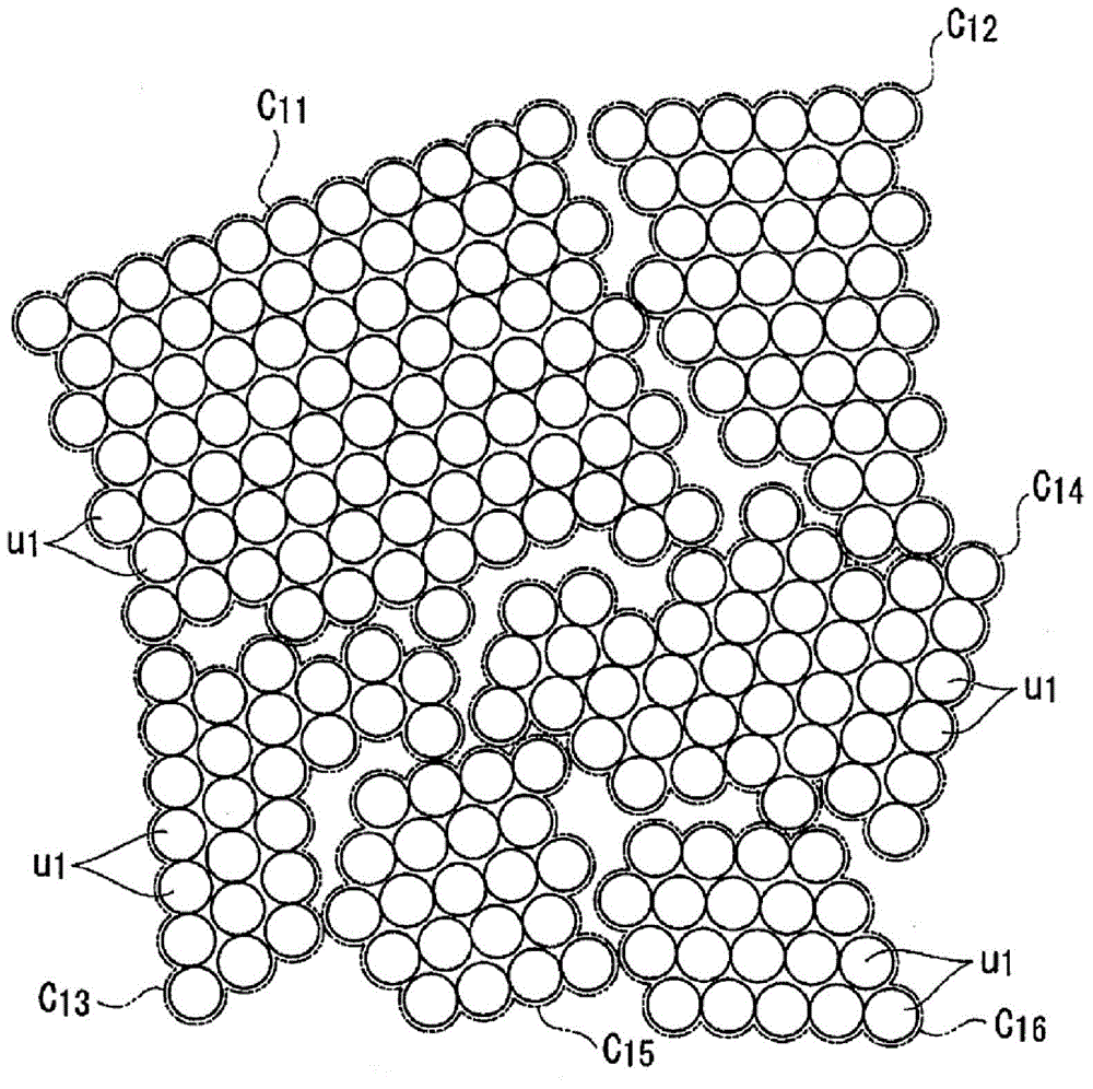
[0109] The concavo-convex structure on the surface of the substrate includes a plurality of protrusions c11 to c1n. Moreover, flat surfaces f11-f1n are formed between each convex part.

[0110] figure 1 t11 to t1n in are the center points of the respective convex portions c11 to c1n. Based on the measurement results of AFM (Atomic Force Microscopy, Atomic Force Microscopy), a plurality of contour lines with a diameter of 20 nm are drawn for each convex part parallel to the reference plane, and the center of gravity of each contour line is obtained (from the x-coordinate and y-coordinate decision point). The average position of each center of gravity (the p...

no. 2 Embodiment approach

[0284] refer to Figure 6 to Figure 13 One embodiment of the semiconductor light emitting element substrate, the semiconductor light emitting element, the manufacturing method of the semiconductor light emitting element substrate, and the semiconductor light emitting element manufacturing method of the present embodiment will be described.

[0285] [Substrates for semiconductor light emitting devices]

[0286] Such as Figure 6 As shown, the substrate for a semiconductor light emitting element (hereinafter referred to as an element substrate 211B) includes a light emitting structure forming surface 211S as one side surface. In the manufacturing process of the semiconductor light emitting element, a light emitting structure is formed on the light emitting structure forming surface 211S.

[0287] As a material for forming the element substrate 211B, the material of the substrate described in the first embodiment can be used. The light emitting structure forming surface 211S i...

Embodiment 1

[0355]

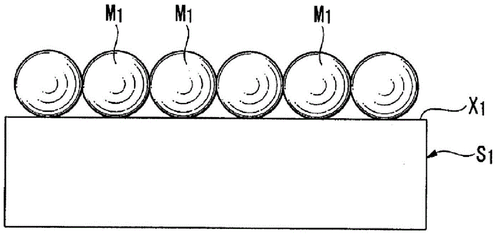
[0356] On a sapphire substrate with a diameter of 2 inches and a thickness of 0.42 mm, SiO with a diameter of 3 μm is coated in a single layer by the single-layer coating method disclosed in Japanese Patent Application No. 2008-522506 2 Colloidal silica particles.

[0357] Specifically, prepare SiO with an average particle size of 3.02 μm 2 A 3.0% by mass aqueous dispersion (dispersion liquid) of spherical colloidal silica particles (coefficient of variation in particle size=0.85%) of colloidal silica particles.

[0358] Then, cetyltrimethylammonium bromide (surfactant) with a concentration of 50% by mass was added to the dispersion liquid so as to become 2.5 mmol / L, and stirred for 30 minutes to make cetyltrimethylammonium bromide Ammonium is adsorbed on the surface of colloidal silica particles. At this time, the dispersion liquid and cetyltrimethylammonium bromide were mixed so that the mass of cetyltrimethylammonium bromide became 0.04 times the mass of the co...


PUM

PropertyMeasurementUnit
Lengthaaaaaaaaaa
Lengthaaaaaaaaaa
Thicknessaaaaaaaaaa

Abstract

This method for manufacturing a semiconductor light emitting element comprises: a particle arranging step wherein a plurality of particles (M) are arranged in a single layer on a substrate (S); a particle etching step wherein spaces are formed among the particles (M) by dry etching the arranged plurality of particles (M) under such conditions that the particles (M) are etched but the substrate (S) is not substantially etched; and a substrate etching step wherein the substrate (S) is dry etched using the plurality of particles (M1) after the particle etching step as an etching mask, thereby forming a recessed and projected structure on one surface (X) of the substrate (S).

Description

technical field [0001] The present invention relates to a substrate for a semiconductor light emitting element, a semiconductor light emitting element, and a method for manufacturing the same. In particular, it relates to a substrate for a semiconductor light-emitting element suitable for a III-V nitride semiconductor light-emitting element, a semiconductor light-emitting element using the substrate obtained by the method, and a method for manufacturing the same. [0002] This case claims priority based on Japanese Patent Application No. 2012-182302 filed in Japan on August 21, 2012 and Japanese Patent Application No. 2013-126025 filed in Japan on June 14, 2013, and its contents are cited here. Background technique [0003] The semiconductor light emitting element is used as an ultraviolet, blue, or green light emitting diode element, or an ultraviolet, blue, or green laser diode element. In particular, a Group III-V nitride semiconductor light-emitting device having a lig...

Claims


Application Information

Patent Timeline
IPC IPC(8): H01L33/22H01L21/3065
CPCH01L21/3065H01L33/22H01L2933/0008H01L2933/0033H01L21/0237H01L21/0242H01L21/0243H01L21/02521H01L21/0254H01L21/0262H01L21/02658H01L21/3081H01L21/3086H01L33/007H01L33/20H01L21/02019H01L21/02282H01L21/02285H01L33/0066H01L33/50H01L2933/0025
Inventor 八田嘉久篠塚启大纮太郎梶田康仁
Owner OJI HLDG CORP
Why Eureka
Try Eureka