Semiconductor light-emitting element and method for producing same
a technology of electromagnetic light and semiconductors, applied in the direction of semiconductor devices, basic electric elements, electrical appliances, etc., can solve the problems of deteriorating light extraction efficiency, total reflection of light, and inability to extract light incident at critical angles or greater to the outside, so as to prevent reflected light, improve light extraction efficiency, and suppress light loss
- Summary
- Abstract
- Description
- Claims
- Application Information
AI Technical Summary
Benefits of technology
Problems solved by technology
Method used
Image
Examples
example 1
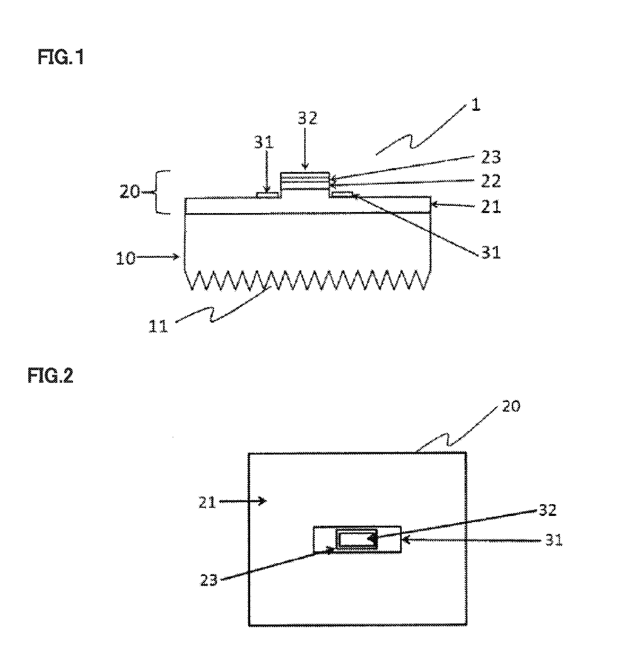
[0065]An n-type AlGaN layer, an active layer (light-emitting layer), and a p-type GaN were successively epitaxially grown on a single-crystal AlN substrate, which had been produced by an HVPE method, by an MOCVD method to obtain an ultraviolet light-emitting element wafer. The compositions were adjusted so that the emission wavelength was 265 nm.
[0066]An etching mask was formed on the wafer, and the region not covered with the etching mask was etched by an inductively coupled plasma (ICP) etching to partially expose the n-type semiconductor layer. Thereafter, an n-type electrode formed of Ti / Al / Au was formed on a part of the exposed portion of the n-type AlGaN layer, and then a p-type electrode formed of Ni / Au was sequentially formed on the p-type GaN layer. Then, a pad layer formed of Ti / Ni / Au was formed on the n-type electrode and the p-type electrode. Thereafter, the back surface of the AlN substrate was mechanically polished to obtain a wafer thickness of 100 μm.
[0067]In the pla...
examples 2 to 4
, Comparative Examples 1 to 4
[0072]An ultraviolet light-emitting element was produced and the optical output of the ultraviolet light-emitting element was measured with a photodiode in the same manner as that in Example 1 except that the electrodes were laid out under the conditions of Table 1 for the exposed area of the n-type semiconductor layer in the area of the ultraviolet light-emitting element, and the exposed areas of p-type contact layer and the p-type electrode. The results are shown in Table 1.
TABLE 1Exposed areas of p-typecontact layer and p-typeOpticaln-typen-typep-typep-typeelectrode in theoutputAlGaN layerElectrodeElectrodeContact Layerremaining arearatioExample 187.1%6.7%5.4%0.8%48.1%2.13Example 280.4%13.4%5.4%0.8%31.6%2.07Example 373.8%20.1%5.4%0.8%23.7%2.06Example 466.2%27.7%5.4%0.8%18.3%2.02Comparative2.7%6.7%5.4%85.2%93.1%1.4Example 1Comparative2.9%13.4%5.4%78.3%86.2%1.45Example 2Comparative3.1%20.1%5.4%71.5%79.4%1.47Example 3Comparative3.2%27.7%5.4%63.7%71.4%1.5...
PUM
 Abstract
Description
Claims
Application Information
