
Eureka
For R&D, Eureka makes reading and utilizing patents & technical documents easy.
Eureka AIR
Designed for self-driven R&D workflows. Generate viable solutions, solve complex R&D challenges, empower your innovation with AI.

Eureka Materials
Designed for material experts only. Revolutionize your material R&D, from search, analyze, to developing new materials.

TechResearch
Generate reliable direction feasibility study reports for your R&D in just a few steps.

TechSeek
Discover and master advanced knowledge NOW. Basics, ideas, possibilities, all at once.

TechMind
As an expert in R&D Theories, TechMind can generates customized viable solutions instantly.

TechRisk
Analyze your overall solution with one click, know your potential R&D risks in advance.

TechMonitor
Get weekly tech updates, stay abreast of the latest tech innovations and key insights.
Resin composition and semiconductor device
a technology of composition and semiconductor, applied in the direction of semiconductor devices, solid-state devices, basic electric elements, etc., can solve problems such as narrowing the gap, and achieve the effect of high reliability
- Summary
- Abstract
- Description
- Claims
- Application Information
AI Technical Summary
Benefits of technology
Problems solved by technology
Method used
Image

Examples
examples
[0066]The present invention will be described with reference to examples. However, the present invention is not limited thereto. In the following examples, parts and percentages are by mass unless otherwise indicated.
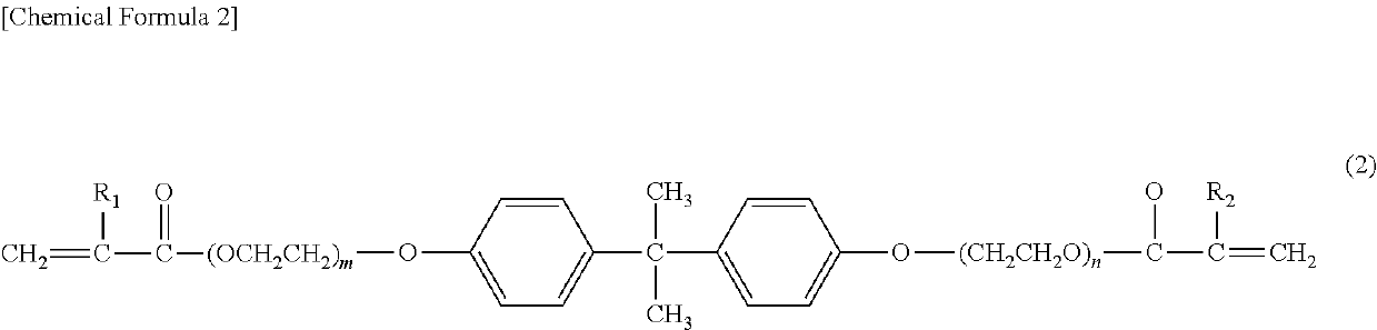
[0067]As the component (A), BPE-80N (EO-modified bisphenol A dimethacrylate manufactured by Shin-Nakamura Chemical Co., Ltd., m+n=2.3 in the general formula (2)), BPE-1300N (EO-modified bisphenol A dimethacrylate manufactured by Shin-Nakamura Chemical Co., Ltd., m+n=30 in the general formula (2)), BPE-200 (EO-modified bisphenol A dimethacrylate manufactured by Shin-Nakamura Chemical Co., Ltd., m+n=4 in the general formula (2)), A-BPE-4 (EO-modified bisphenol A diacrylate manufactured by Shin-Nakamura Chemical Co., Ltd., m+n=4 in the general formula (2)), and Viscoat #540 (bisphenol A diacrylate manufactured by Osaka Organic Chemical Industry Ltd.) were used. As the component (B), A-DCP (tricyclodecanedimethanol diacrylate manufactured by Shin-Nakamura Chemical Co., Ltd....
examples 1 to 18
, Comparative Examples 1 to 5
[0068]With formulations shown in Tables 1 to 3, the components (A) to (F) were mixed using the three-roll mill to prepare the resin composition.
[Initial Evaluation]
>
[0069]A test silicon chip (Si size: 7.3 mm×7.3 mm×0.125 mm thick, bump size: solder layer formed on a Cu pillar of 30 μm×30 μm×30 μm, number of bumps: 544) and an organic substrate (substrate size: 187.5 mm×64.0 mm×0.36 mm thick, electrode: OSP (Organic Solderability Preservative) treated Cu pillar) for mounting the test chip were used. Shapes of the silicon chip and the Cu pillar were cubes. When the test silicon chip and the substrate are joined using flux, a value between resistance value measurement pads was 28 to 32Ω. When a connection surface between the test silicon chip and the substrate was observed, sufficient solder wetting was confirmed in all the bumps. Therefore, this value was taken as a reference value.
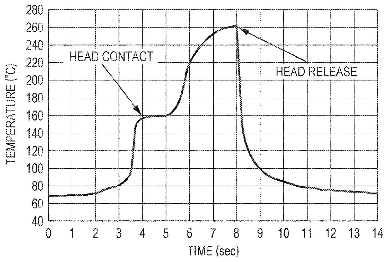
[0070]The prepared resin composition was applied on the organic substrate i...
PUM
| Property | Measurement | Unit |
|---|---|---|
| particle diameter | aaaaa | aaaaa |
| particle diameter | aaaaa | aaaaa |
| particle diameter | aaaaa | aaaaa |
Abstract
Description
Claims
Application Information
 - R&D Engineer
- R&D Manager
- IP Professional
- Industry Leading Data Capabilities
- Powerful AI technology
- Patent DNA Extraction
Browse by: Latest US Patents, China's latest patents, Technical Efficacy Thesaurus, Application Domain, Technology Topic, Popular Technical Reports.
© 2024 PatSnap. All rights reserved.Legal|Privacy policy|Modern Slavery Act Transparency Statement|Sitemap|About US| Contact US: help@patsnap.com