Semiconductor device having a stacked electrode with an electroless nickel plating layer

a technology of nickel plating and stacked electrodes, applied in the direction of semiconductor devices, semiconductor/solid-state device details, electrical equipment, etc., can solve the problems of affecting increasing leakage current, so as to improve the reliability of power conversion apparatus, reduce the size, and high reliability

Active Publication Date: 2020-11-24
HITACHI POWER SEMICON DEVICE
View PDF17 Cites 0 Cited by
  • Summary
  • Abstract
  • Description
  • Claims
  • Application Information

AI Technical Summary

Benefits of technology

[0015]Therefore, an object of the present invention is to provide a highly reliable semiconductor device which has an electrode including an electroless Ni plating layer and in which a crack is hardly generated in the electroless Ni plating layer, and a manufacturing method thereof.
[0018]According to the present invention, it is possible to realize the highly reliable semiconductor device which has the electrode including the electroless Ni plating layer and in which the crack is hardly generated in the electroless Ni plating layer, and the manufacturing method thereof.
[0019]As a result, it is possible to reduce a size and increase reliability of a power conversion apparatus on which the semiconductor device is mounted.

Problems solved by technology

As a result of studies conducted by the inventors of the present application, however, it has been found that a crack is likely to occur depending on a type of an electroless Ni plating bath and a heat treatment condition after plating deposition even in the case where the phosphorus concentration is equal to or higher than 4 wt % and lower than 6 wt % as in JP 2015-56532 A. If a crack is generated in the electroless Ni plating film, there is a possibility that the crack may develop depending on a temperature and stress change to cause characteristic defects.
When a semiconductor chip is electrically connected to a connection terminal using a junction layer formed of a copper sintered layer, copper diffuses from the junction layer to the power semiconductor chip if a crack is generated in an electroless Ni plating electrode of the semiconductor chip, and there are problems that an element leak current increases, an element withstand voltage deteriorates, and characteristics of the element fluctuate.

Method used


Image

  • Semiconductor device having a stacked electrode with an electroless nickel plating layer
  • Semiconductor device having a stacked electrode with an electroless nickel plating layer
  • Semiconductor device having a stacked electrode with an electroless nickel plating layer

Examples


first embodiment

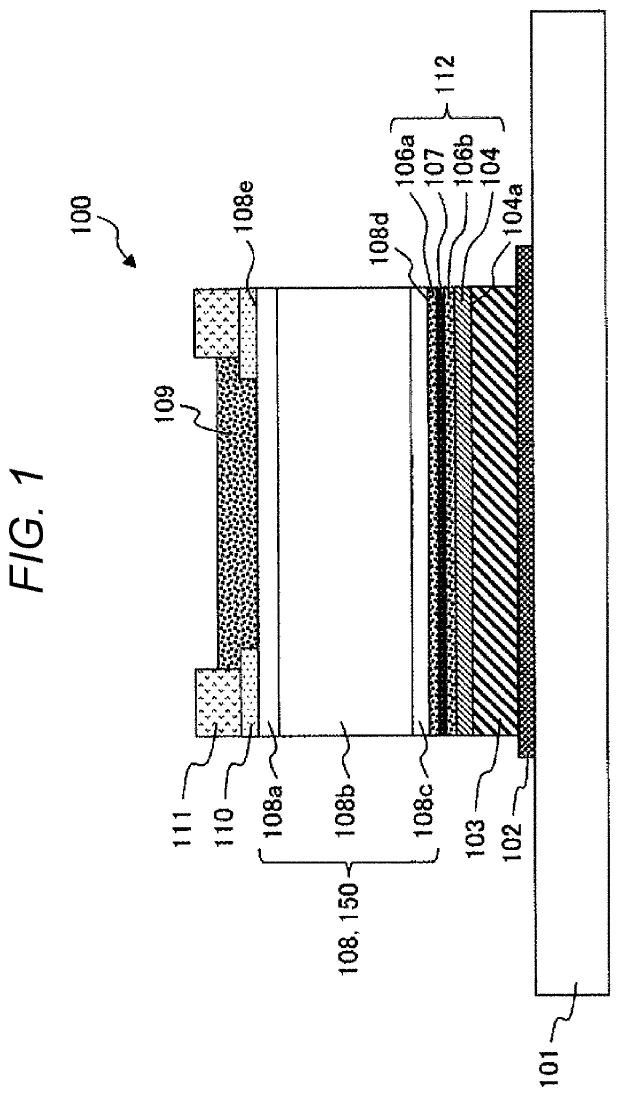
[0041]A semiconductor device and a manufacturing method thereof according to a first embodiment of the present invention will be described with reference to FIGS. 1 to 15. FIG. 1 is a cross-sectional view of the semiconductor device according to the first embodiment of the present invention, and illustrates a sectional structure in the case of being applied to a freewheel diode of a power semiconductor chip. Although a description will be given assuming a diode using an n type Si substrate hereinafter, the invention is not limited thereto. Even when a p type Si substrate is used, the invention can be handled in the same manner. Further, the invention can be handled in the same manner in an electrode structure of an IGBT that causes a current to flow in the vertical direction. Further, the invention can be handled in the same manner regarding a wide-gap semiconductor such as SiC, GaN, and GaO.

[0042]As illustrated in FIG. 1, a semiconductor device 100 of the embodiment includes a semi...

second embodiment

[0090]A semiconductor device and a manufacturing method thereof according to a second embodiment of the present invention will be described with reference to FIGS. 16A and 16B. FIG. 16A is a cross-sectional view of a semiconductor device 200 according to the second embodiment of the present invention. FIG. 16B is a cross-sectional view of the semiconductor device 200 in FIG. 16A after wire bonding.

[0091]The semiconductor device 200 of the present embodiment is an example of the case of being applied to a freewheel diode of a power semiconductor chip similarly to the first embodiment. Although a description will be given assuming a diode using an n type Si substrate hereinafter, the invention is not limited thereto. Even when a p type Si substrate is used, the invention can be handled in the same manner. Further, the invention can be handled in the same manner in an electrode structure of an IGBT that causes a current to flow in the vertical direction. Further, the invention can be h...

third embodiment

[0100]A semiconductor device and a manufacturing method thereof according to a third embodiment of the present invention will be described with reference to FIG. 17. FIG. 17 is a cross-sectional view of a semiconductor device 300 according to the third embodiment of the present invention.

[0101]The semiconductor device 300 of the present embodiment is an example of the case of being applied to a freewheel diode of a power semiconductor chip similarly to the first embodiment. Although a description will be given assuming a diode using an n type Si substrate hereinafter, the invention is not limited thereto. Even when a p type Si substrate is used, the invention can be handled in the same manner. Further, the invention can be handled in the same manner in an electrode structure of an IGBT that causes a current to flow in the vertical direction. Further, the invention can be handled in the same manner regarding a wide-gap semiconductor such as SiC, GaN, and GaO.

[0102]As illustrated in F...


PUM

PropertyMeasurementUnit
voltageaaaaaaaaaa
thicknessaaaaaaaaaa
thicknessaaaaaaaaaa

Abstract

A semiconductor device including: a semiconductor element; and a first electrode formed on a first surface of the semiconductor element. The first electrode has a stacked structure including a first electroless Ni plating layer. The first electroless Ni plating layer contains nickel (Ni) and phosphorus (P) as a composition. A phosphorus (P) concentration of the first electroless Ni plating layer is 2.5 wt % to 6 wt % inclusive, and a crystallization rate of Ni3P in the first electroless Ni plating layer is 0% to 20% inclusive.

Description

CLAIM OF PRIORITY[0001]The present application claims priority from Japanese Patent application serial no. 2018-159171, filed on Aug. 28, 2018, the content of which is hereby incorporated by reference into this application.BACKGROUND OF THE INVENTION1. Field of the Invention[0002]The present invention relates to a structure of a semiconductor device and a manufacturing method thereof, and particularly to a technique advantageous for miniaturization and high reliability of a power conversion apparatus on which a semiconductor device is mounted.2. Description of the Related Art[0003]Semiconductor devices have been used in a wide range of fields such as system large scale integration (LSI), power conversion apparatuses, and control devices for hybrid vehicles. In such semiconductor devices, “solder” or a “solder alloy” containing lead has been mainly used, for example, for electrical junction between an electrode terminal of an electronic component and an electrode terminal of a circui...

Claims


Application Information

Patent Timeline
Patent Type & Authority Patents(United States)
IPC IPC(8): H01L29/08H01L23/00H01L29/739H01L29/73H01L21/288
CPCH01L29/7397H01L24/33H01L21/288H01L29/0834H01L2924/01028H01L2924/01029H01L29/456H01L29/861H01L2224/06181H01L2224/04042H01L2224/04026H01L2224/8384H01L2224/32238H01L2224/05083H01L2224/05023H01L2224/05568H01L2224/0345H01L2224/03464H01L2224/29H01L2224/05001H01L2224/0554H01L2224/83203H01L2224/83065H01L2224/05019H01L2224/05559H01L24/05H01L24/06H01L24/03H01L24/48H01L24/32H01L2224/45124H01L2224/73265H01L29/401H01L21/28512H01L29/417H01L29/7395H01L2924/3511H01L2224/05166H01L2224/83447H01L2224/05186H01L2224/05155H01L2224/85447H01L2224/29199H01L2224/29347H01L2224/05138H01L2224/45324H01L2224/05184H01L2224/29147H01L2224/05124H01L2924/00014H01L2924/00013H01L2924/013H01L2924/01015H01L2924/01022H01L2924/01014H01L2924/01074H01L2924/01013H01L2924/04941
Inventor FURUKAWA, TOMOYASUMORITA, TOSHIAKIKAWASE, DAISUKETABATA, TOSHIHITO
Owner HITACHI POWER SEMICON DEVICE
Why Eureka
Try Eureka