Eureka AIR delivers breakthrough ideas for toughest innovation challenges, trusted by R&D personnel around the world.

Display panel comprising a photosensitive component that receives reflected light of a fingerprint and is connected to an underside of a second thin film transistor layer and display device

Active Publication Date: 2021-01-05
WUHAN CHINA STAR OPTOELECTRONICS TECH CO LTD
View PDF13 Cites 0 Cited by
  • Summary
  • Abstract
  • Description
  • Claims
  • Application Information

AI Technical Summary

Benefits of technology

The present patent provides a display panel and a display device that includes a color filter on array process on the display substrate, and a photosensitive component for fingerprint sensing. The technical effect of this invention is to improve the sensitivity of fingerprint recognition on the display panel, and to provide a better unlocking experience for people. The photosensitive component is disposed on the light-emitting surface of the counter substrate, which shortens the distance between the photosensitive component and the finger fingerprint, reducing the loss of reflected light of the fingerprint. Additionally, the display panel includes a pixel definition layer with a plurality of pixel regions, and a detection light source emitting a reflected light when the user touches the display panel.

Problems solved by technology

For example, the traditional optical sensor method cannot achieve thinness and light weight, especially in the case of high resolution, the conventional device is bulky and cannot be portable, so it is difficult to integrate into a device such as a mobile phone.
Although other methods solve the problem of thinness and light weight, they cannot realize a larged-area array, or cannot combine other functions, and the process is complicated and costly.
However, the divergence of the divergent light reflected by the valleys and ridges of the finger fingerprint is poor and the difference in light energy is extremely small, and there is also interference of ambient light between the valleys and the ridges of the finger fingerprint, so it is difficult to accurately perform the fingerprint recognition.

Method used


Image

  • Display panel comprising a photosensitive component that receives reflected light of a fingerprint and is connected to an underside of a second thin film transistor layer and display device
  • Display panel comprising a photosensitive component that receives reflected light of a fingerprint and is connected to an underside of a second thin film transistor layer and display device
  • Display panel comprising a photosensitive component that receives reflected light of a fingerprint and is connected to an underside of a second thin film transistor layer and display device

Examples


Embodiment Construction

[0038]The preferred embodiments of the present disclosure are described below with reference to the accompanying drawings, which are used to exemplify the disclosure. The technical content of the present disclosure makes the technical content of the present disclosure clearer and easier to understand. However, the present disclosure can be embodied in many different forms of embodiments, and the scope of the disclosure is not limited to the embodiments mentioned herein.

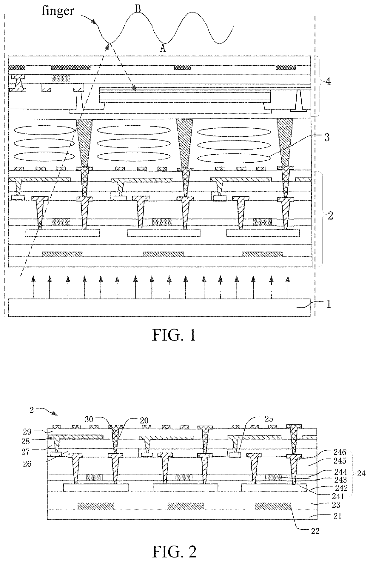
[0039]An embodiment of the present invention provides a display panel, which realizes optical fingerprint recognition through a display substrate and a counter substrate, and the display substrate is a color filter on array (COA) which adopts a technique of color film on array, an aperture ratio of display substrate can be increased. Moreover, the photosensitive component is disposed on the counter substrate, which can accurately recognize the divergence of valleys and ridges of the finger fingerprint and the differen...


PUM


Abstract

A display panel and a display device are provided, which the display panel including a display substrate, a counter substrate, and a backlight. The display substrate includes a first thin film transistor layer, a touch electrode, and a pixel definition layer. The substrate includes a second thin film transistor layer and a photosensitive component. The second thin film transistor layer has a plurality of thin film transistors. The photosensitive component is connected to an underside of the second thin film transistor layer. The photosensitive component receives a reflected light of a user's fingerprint to identify an identification of the user.

Description

FIELD OF INVENTION[0001]The present disclosure relates to the field of displays, and in particular, to a display panel and a display device.BACKGROUND OF INVENTION[0002]Fingerprint recognition as a biometric recognition method has recently attracted widespread attention, especially in mobile payment. Many methods of fingerprint recognition have also been invented, such as optical, capacitive, microwave, temperature, and ultrasonic. However, each approach has its advantages and disadvantages. For example, the traditional optical sensor method cannot achieve thinness and light weight, especially in the case of high resolution, the conventional device is bulky and cannot be portable, so it is difficult to integrate into a device such as a mobile phone. Although other methods solve the problem of thinness and light weight, they cannot realize a larged-area array, or cannot combine other functions, and the process is complicated and costly.[0003]In the conventional art, a medical use of ...

Claims


Application Information

Patent Timeline
IPC IPC(8): G02F1/133G02F1/1333G02F1/1362
CPCG02F1/13318G02F1/13338G02F1/136209G02F1/136227G02F2001/13312G02F1/13312
Inventor XIAO, JUNCHENGAI, FEIYAN, YUAN
Owner WUHAN CHINA STAR OPTOELECTRONICS TECH CO LTD
Why Eureka
Eureka Blog
Learn More