

Wireless communication semiconductor integrated circuit device and wireless communication system
- Summary
- Abstract
- Description
- Claims
- Application Information
AI Technical Summary
Benefits of technology
Problems solved by technology
Method used
Image

Examples
Embodiment Construction
[0031] Preferred embodiments of the present invention will hereinafter be described in detail with reference to the accompanying drawings.
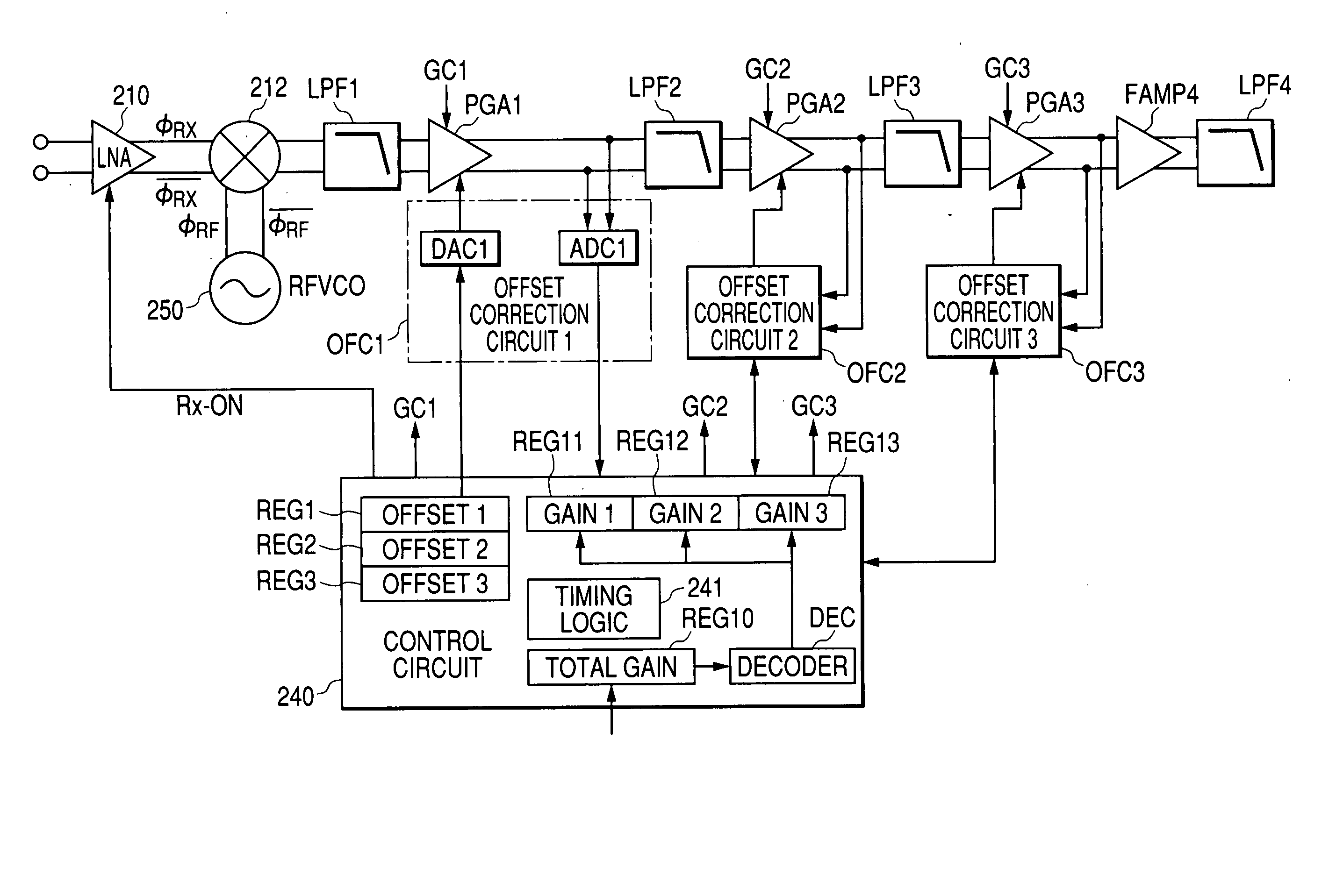
[0032] A reception system circuit of a direct conversion system employed in a wireless communication system of a cellular phone or the like suitable for application of the present invention is shown in FIG. 1.
[0033] The reception system circuit according to the present embodiment comprises an LNA (Low Noise Amplifier) 210 which amplifies a received signal, an oscillator 250 which generates a local oscillation signal φRF, a mixer 212 which combines the received signal amplified by the LNA 210 and the local oscillation signal φRF generated by the oscillator 250 and down-converts the result of combination to a signal lying in an audio frequency band, and a high gain amplifier circuit 220 which amplifies the down-converted signal.
[0034] In the high gain amplifier circuit 220, a first variable gain amplifier (programmable gain amplifier) PGA1 is con...
PUM
 Abstract
Description
Claims
Application Information