Ultrasonic sensor and manufacture method of the same
- Summary
- Abstract
- Description
- Claims
- Application Information
AI Technical Summary
Benefits of technology
Problems solved by technology
Method used
Image
Examples
embodiments
First Embodiment
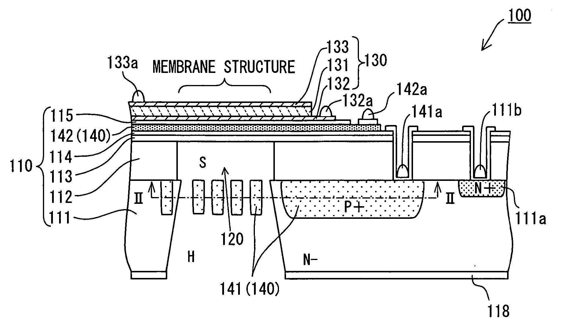
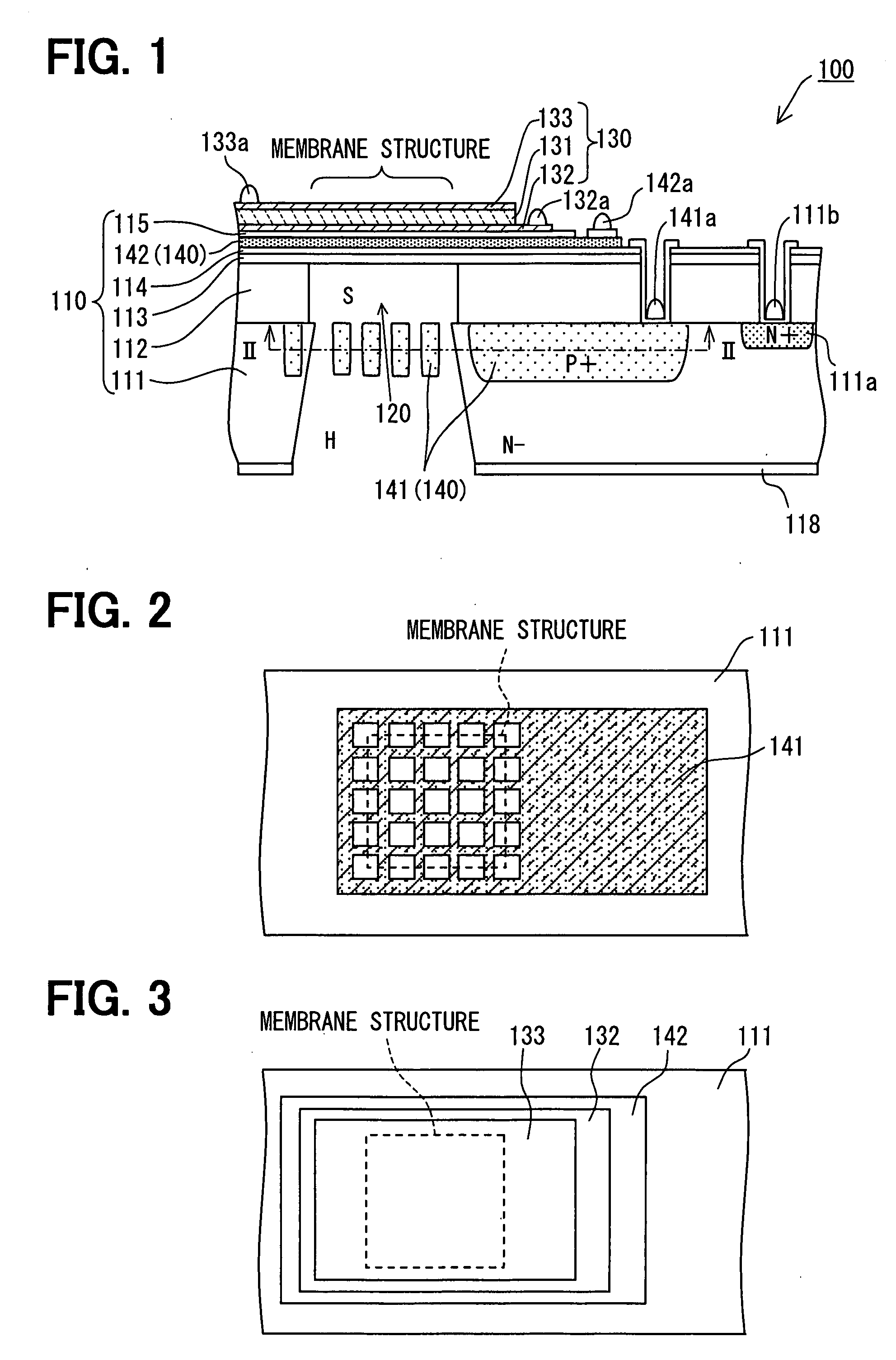
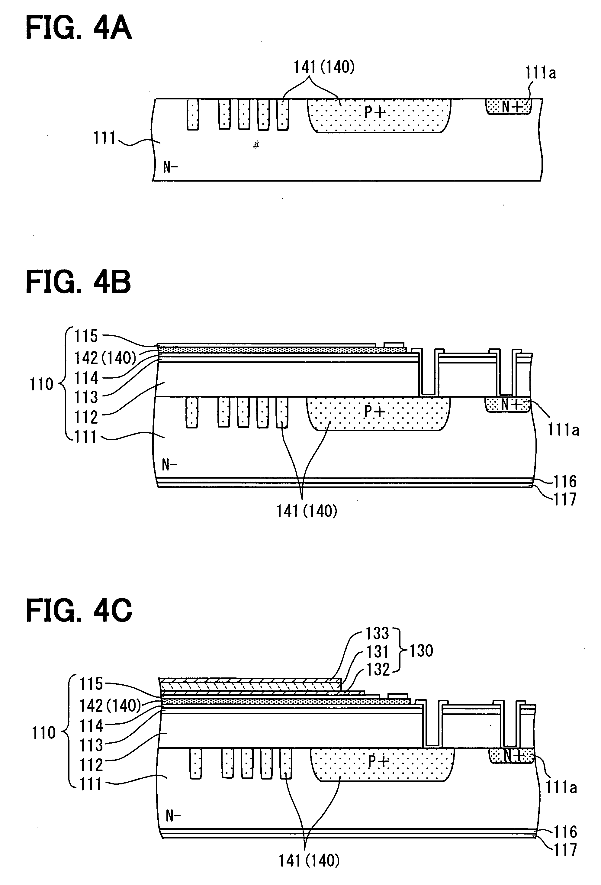
[0045] An ultrasonic sensor 100 according to a first embodiment of the present invention will be described with reference to FIGS. 1-5B. As shown in FIG. 1, the ultrasonic sensor 100 can be a piezoelectric type ultrasonic sensor which is manufactured by MEMS technology, for example.
[0046] The ultrasonic sensor 100 has a substrate unit 110, a piezoelectric oscillator 130 which is arranged at a thin-walled portion 120 of the substrate unit 110, and an adjustment electrode unit 140 for applying a predetermined voltage to the thin-walled portion 120. In this case, the adjustment electrode unit 140 includes a first adjustment electrode 141 and a second adjustment electrode 142.
[0047] The substrate unit 110 includes a semiconductor substrate 111 (semiconductor-on-insulator substrate) of a first conductivity type. In this embodiment, the semiconductor substrate 111 is constructed of a N-typed silicon substrate of a (100) plane orientation. The first adjustment electrode ...
second embodiment
[0094] Next, a second embodiment of the present invention will be described with reference to FIGS. 7-9B.
[0095] As shown in FIG. 7, the ultrasonic sensor 100 can be constructed of the ultrasonic sensor of the piezoelectric type which is manufactured by the MEMS technology. The ultrasonic sensor 100 includes the substrate unit 110, the piezoelectric oscillator 130 formed at the thin-walled portion 120 of the substrate unit 110 and the adjustment electrode unit 140 for applying the predetermined voltage to the thin-walled portion 120. The adjustment electrode unit 140 has the first adjustment electrode 141 and the second adjustment electrode 142.
[0096] The substrate unit 110 has the semiconductor substrate 111 where a semiconductor layer 211c is arranged at a support substrate 211b through an embedded insulating membrane 211a (silicon oxidation membrane). Dopant impurity (e.g., boron which is used in this embodiment) is introduced into the semiconductor layer 211c, and the semicondu...
third embodiment
[0117] A third embodiment of the present invention will be described with reference to FIGS. 10-12C.
[0118] As shown in FIG. 10, the ultrasonic sensor 100 can be a piezoelectric type ultrasonic sensor which is manufactured by the MEMS technology. The ultrasonic sensor 100 has the substrate unit 110, the piezoelectric oscillator 130 which is arranged at the thin-walled portion 120 of the substrate unit 110, and the adjustment electrode unit 140 for applying the predetermined voltage to the thin-walled portion 120. According to the third embodiment, the adjustment electrode unit 140 has the first adjustment electrode 141 and the second adjustment electrode 142 which is also used as the lower detection electrode 132 of the piezoelectric oscillator 130.
[0119] Similarly to the first embodiment, the substrate unit 110 includes the semiconductor substrate 111 of the first conductive type. In this case, the semiconductor substrate 111 is constructed of the N-typed silicon substrate of the ...
PUM
 Abstract
Description
Claims
Application Information


