Electronic device and electronic device manufacturing method

a manufacturing method and electronic device technology, applied in the direction of telephone set construction, switch side location, hermetically sealed casing, etc., can solve the problem of hard to apply all parts, and achieve the effect of simplifying the type of product, reducing manufacturing costs, and reducing manufacturing costs

Active Publication Date: 2021-02-02
SAMSUNG ELECTRONICS CO LTD
View PDF15 Cites 2 Cited by
  • Summary
  • Abstract
  • Description
  • Claims
  • Application Information

AI Technical Summary

Benefits of technology

[0010]According to various embodiments of the present invention, in an electronic device including a key module, washers, O-rings, or other parts may be integrally formed and placed with other components, simplifying the type of product and resolving limitations in the mounting space and hence leading to cost savings and slim products.
[0011]According to various embodiments of the present invention, a uni-body key module structure may achieve key waterproof / anti-dust capability with a simplified structure while preventing the side key from wiggling, along with securing a better click feeling.
[0012]According to various embodiments of the present invention, a uni-body key module structure enables various design implementations that may meet customers' needs by using the mounting space in the electronic device.

Problems solved by technology

However, use of additional parts to secure waterproof capability places a significant limitation on the mounting space of the portable terminal when all of the parts are applied to the terminal and cause problems with key protrusions due to accumulated tolerances.
Especially, it is hard to apply all of the parts to such a structure as a side key, where a washer and spring are difficult to mount.

Method used


Image

  • Electronic device and electronic device manufacturing method
  • Electronic device and electronic device manufacturing method
  • Electronic device and electronic device manufacturing method

Examples


Embodiment Construction

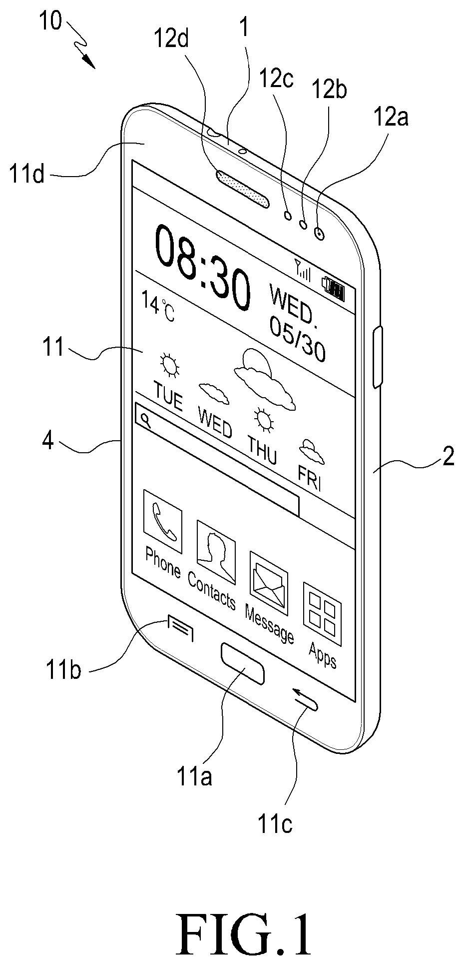
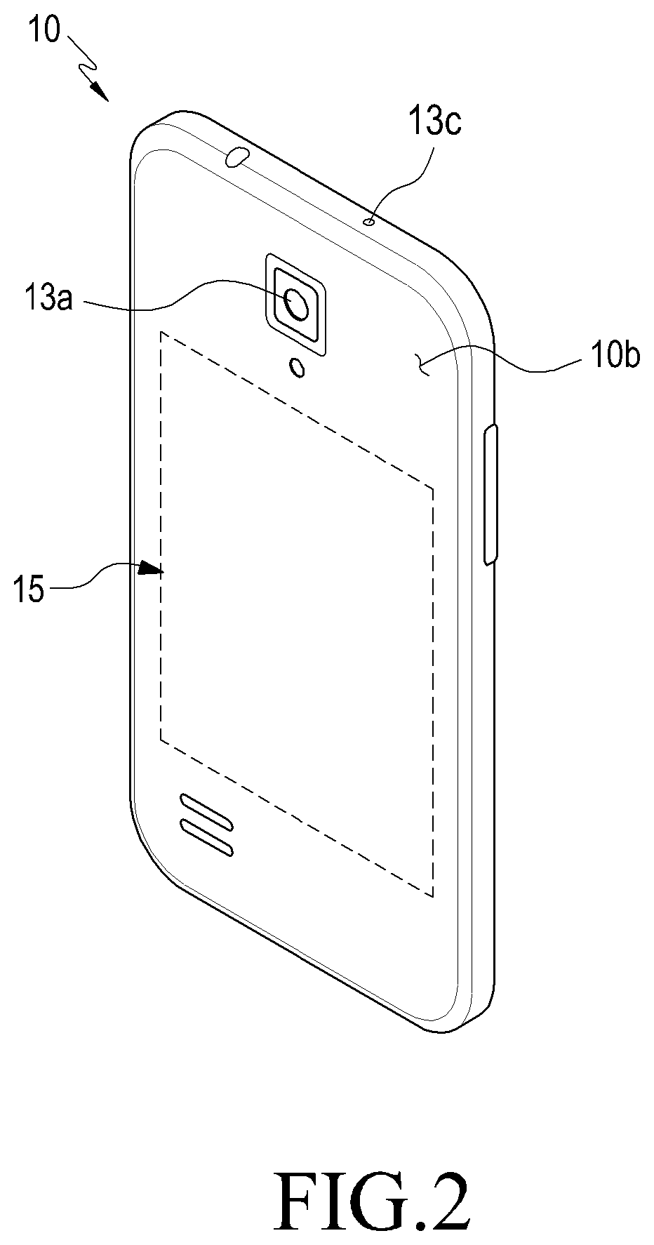
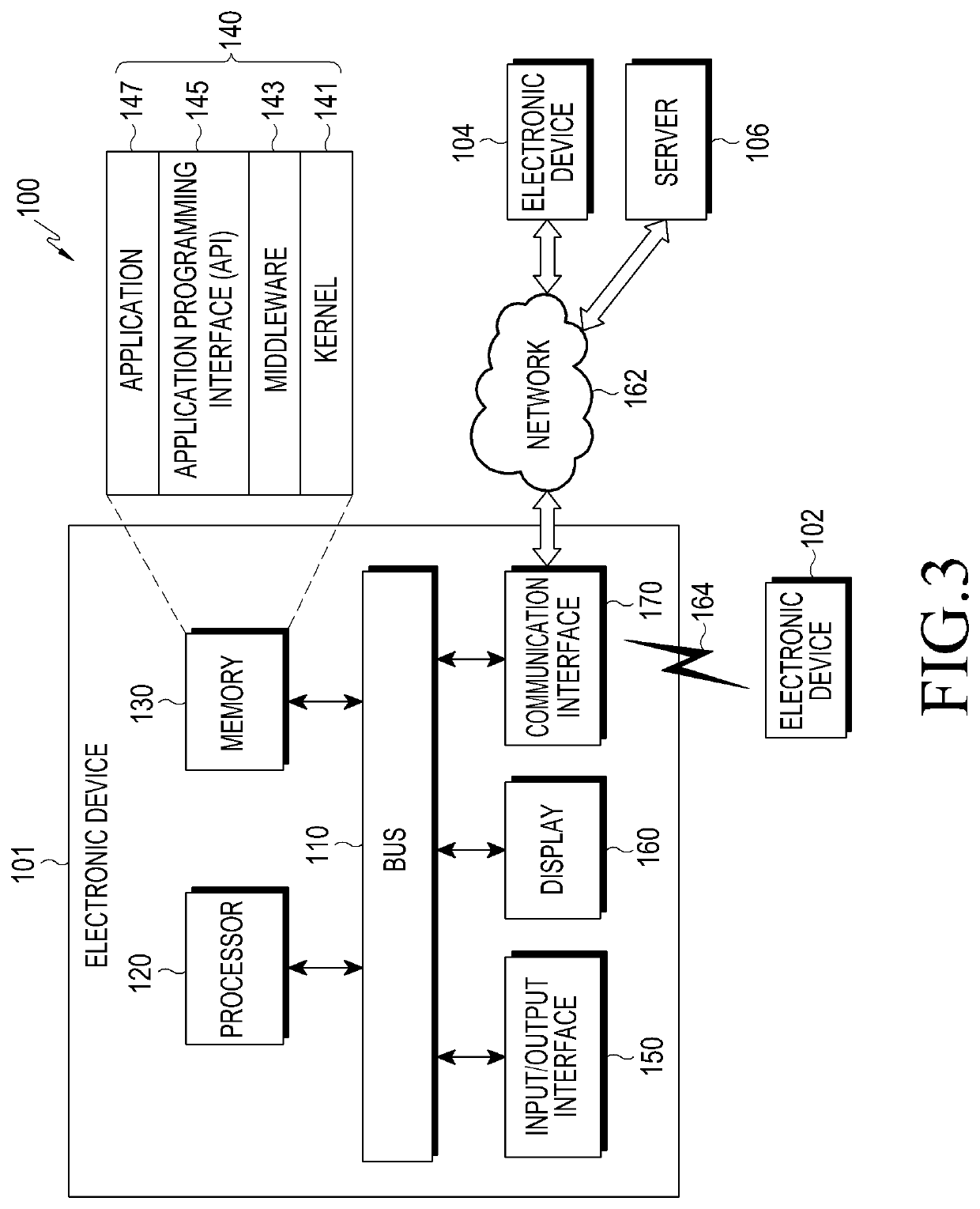
[0032]Hereinafter, embodiments of the present disclosure are described with reference to the accompanying drawings. However, it should be appreciated that the present disclosure is not limited to the embodiments, and all changes and / or equivalents or replacements thereto also belong to the scope of the present disclosure. The same or similar reference denotations may be used to refer to the same or similar elements throughout the specification and the drawings.

[0033]As used herein, the terms “have,”“may have,”“include,” or “may include” a feature (e.g., a number, function, operation, or a component such as a part) indicate the existence of the feature and do not exclude the existence of other features.

[0034]As used herein, the terms “A or B,”“at least one of A and / or B,” or “one or more of A and / or B” may include all possible combinations of A and B. For example, “A or B,”“at least one of A and B,”“at least one of A or B” may indicate all of (1) including at least one A, (2) includi...


PUM


Abstract

Various embodiments relating to an electronic device including a key module are disclosed, and according to one embodiment, a portable electronic device comprises: a front glass cover defining the front surface of the electronic device; a rear cover defining the rear surface of the electronic device; a bezel surrounding a space defined by the front cover and the rear cover, the bezel being integrally formed with or separately formed from the rear cover, the bezel including a portion including an opening; a display device built in the space and including a screen area exposed through the front cover; and a plate including a plane parallel to the front cover within the space, wherein the opening penetrates from the outside of the bezel toward the space in a first direction. The electronic device comprises: a key having a size and a shape that can pass through the opening, the key being movably inserted in the opening and including a first surface facing the first direction; a support structure mounted on the plate or a portion of the bezel and including a hole through which the key passes; a dome button mounted on the support structure and arranged to face the first surface of the key and the hole so that the key can be pressed when moving in the first direction; and a waterproof structure including a flexible material. The waterproof structure may comprise: a first portion located between the first surface of the key and the dome button; and a second portion extending from the first portion and inserted between the support structure and the bezel, the second portion sealing a space between the support structure and the bezel so as to waterproof the space. Other various embodiments are also possible.

Description

[0001]This application is a National Phase Entry of PCT International Application No. PCT / KR2016 / 008462, which was filed on Aug. 1, 2016 and claims priority under 35 U.S.C. § 119 of Korean Patent Application No. 10-2015-0144974, filed on Oct. 16, 2015, in the Korean Intellectual Property Office and Korean Patent Application No. 10-2016-0020036, filed on Feb. 19, 2016, in the Korean Intellectual Property Office, the disclosure of which is incorporated herein by reference in its entirety.TECHNICAL FIELD[0002]Various embodiments of the present invention relate to key input devices mounted in portable electronic devices and methods for manufacturing key input devices.BACKGROUND ART[0003]Portable terminals with new functionalities are quickly developing, and with them flourishing, portable terminals are becoming important part of human everyday life.[0004]Smartphones or other portable terminals which are commonly used as mobile communication technology evolves are equipped with various k...

Claims


Application Information

Patent Timeline
Patent Type & Authority Patents(United States)
IPC IPC(8): H01H13/06H01H13/86H04M1/23H04M1/18H01H13/14H04M1/02H05K5/06H01H13/48
CPCH01H13/06H01H13/14H01H13/86H04M1/0277H04M1/18H04M1/23H04M1/236H05K5/06H01H13/48H01H2223/002H01H2225/028
Inventor CHOI, JONG-MINJANG, HYUK-JAEKIM, WOONG-CHANKIM, JUNG-TAEPARK, DAE-HYEONGYI, SANG-HYUNLEE, JAE-RYANGJEON, JEONG-GOOCHO, SUNG-GUNCHO, SUNG-JOOCHOI, YOUNG-SIKYANG, SOON-WOONGLEE, MIN-SUNG
Owner SAMSUNG ELECTRONICS CO LTD
Why Eureka
Try Eureka