
Ferroelectric memory device and method of manufacturing the same

a technology of ferroelectric capacitors and ferroelectric memory, which is applied in the direction of digital storage, capacitors, instruments, etc., can solve the problems of not providing detailed description of the hysteresis loop characteristics of ferroelectric capacitors, and the inability to ensure the generally required 10-year guarantee for semiconductors, etc., and achieves simple matrix type ferroelectric memory, and hysteresis loop characteristics

Inactive Publication Date: 2005-07-26
SEIKO EPSON CORP
View PDF13 Cites 18 Cited by
  • Summary
  • Abstract
  • Description
  • Claims
  • Application Information

AI Technical Summary

Benefits of technology

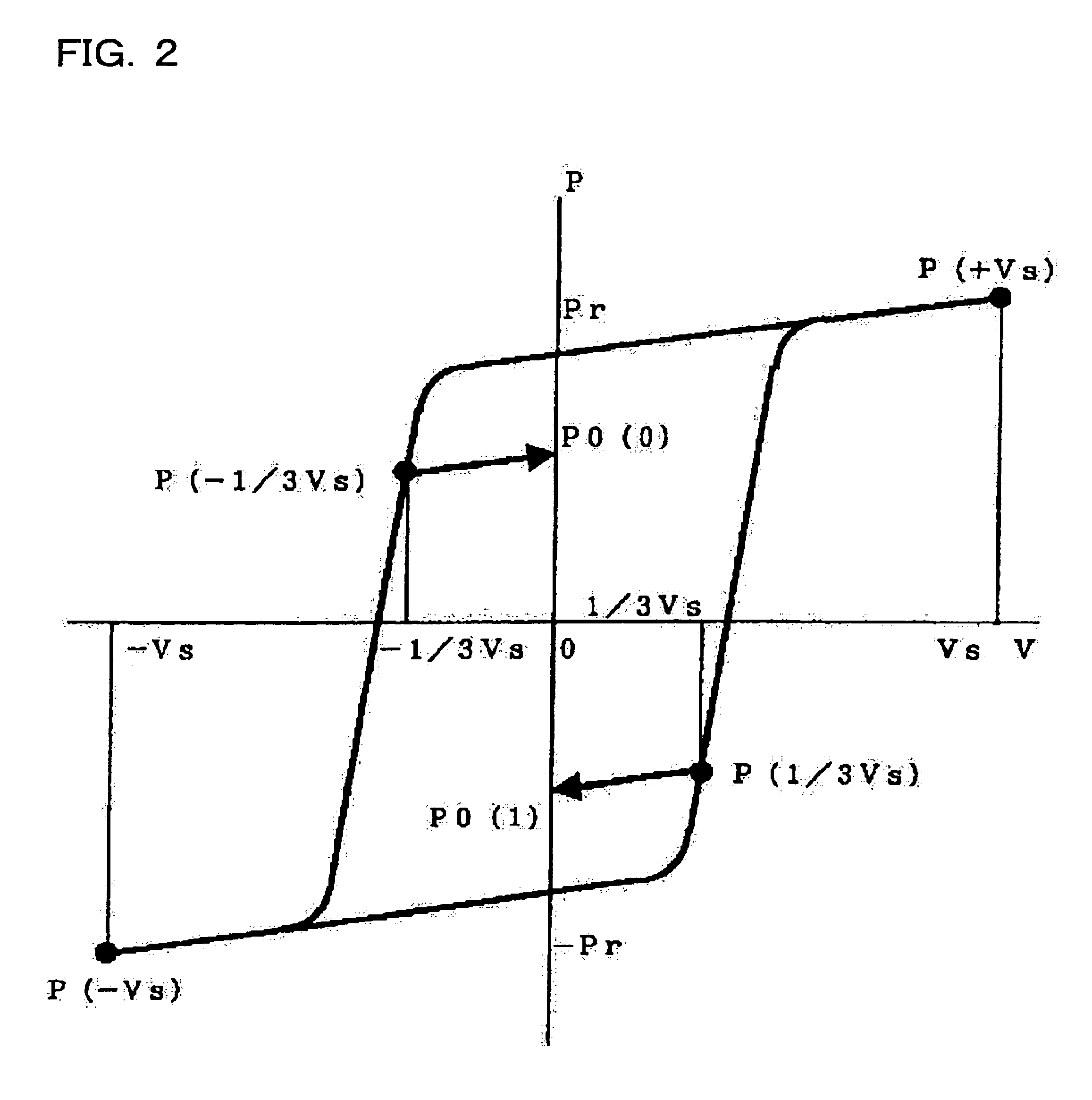
[0005]The present invention may provide a simple matrix type ferroelectric memory device including a ferroelectric capacitor having hysteresis loop characteristics which enable a simple matrix type ferroelectric memory device to be operated in practice, and a method of manufacturing the same.

Problems solved by technology

Therefore, it is considered to be impossible to ensure a 10-year guarantee generally required for semiconductors.
However, this technology does not provide detailed description relating to hysteresis loop characteristics of the ferroelectric capacitor necessary for the operation.

Method used


Image

  • Ferroelectric memory device and method of manufacturing the same
  • Ferroelectric memory device and method of manufacturing the same
  • Ferroelectric memory device and method of manufacturing the same

Examples


first example

[0094]In this exmple, SBT was used as a ferroelectric material. A first raw material liquid for forming a ferroelectric was obtained as follows. 1100 ml of a toluene solution of bismuth 2-ethylhexanoate at a concentration of 0.1 mol / l, 400 ml of a toluene solution of strontium 2-ethylhexanoate at a concentration of 0.1 mol / l, 1000 ml of a toluene solution of tantalum ethoxide at a concentration of 0.1 mol / l, and 100 g of 2-ethylhexane were mixed to prepare a mixed liquid. After refluxing the mixed liquid at 120° C. for one hour in a nitrogen atmosphere, the solvent was evaporated at atmospheric pressure. Toluene was added to the mixture so that the oxide concentration as Sr0.8Bi2.2Ta2Ox (SBT) was 0.1 mol / l to obtain a first raw material liquid.

[0095]A second raw material liquid for forming a paraelectric was obtained as follows. 1500 ml of a toluene solution of bismuth 2-ethylhexanoate at a concentration of 0.1 mol / l, 750 ml of a toluene solution of silicon ethoxide at a concentrati...

second example

[0098]In this example, Bi4W0.1V0.2Si0.1Ge0.1Ti2.5O12 (BWVSGT1) and Bi4W0.2V0.4Si0.2Ge0.2Ti2O12 (BWVSGT2), which are materials in which a Bi-based ferroelectric material Bi4Ti3O12 (BIT) and a paraelectric were mixed, were deposited on a platinum electrode by using a spin coating method.

[0099]A procedure for synthesizing a sol-gel solution in this example is described below. A sol-gel solution for forming a Bi4(W,V,Si,Ge,Ti)3O12 ferroelectric was prepared by mixing a sol-gel solution for forming Bi4Ti3O12 (BIT) and sol-gel solutions for forming WSiO5 (WSO) and V2GeO7 (VGO). WSO and VGO are materials known in the art as layered catalytic oxides.

[0100]A sol-gel solution for forming BWVSGT1 is a solution in which WSO and VGO, 0.1 mol each, were added to 1 mol of the BIT sol-gel solution. A sol-gel solution for forming BWVSGT2 is a solution in which WSO and VGO, 0.2 mol each, were added to 1 mol of the BIT sol-gel solution.

[0101]A Pt coated Si substrate was used as a substrate. Thin films...

third example

[0111]This example relates to a Pb-based ferroelectric material.

[0112]In this example, Pb1.1Zr0.1Ti0.8Si0.1O3 (PZTS1) and Pb1.1Zr0.7Ti0.2Si0.1O3 (PZTS2) were deposited on a platinum electrode by using a spin coating method. A procedure for synthesizing a sol-gel solution in this example is described below. A ferroelectric material was prepared by mixing a sol-gel solution for forming a PbZrTiO3 (PZT) ferroelectric and a sol-gel solution for forming PbSiO3 (PSO).

[0113]Thin films were formed by using solutions in which 0.01 mol of PSO was added to 1 mol of PZT sol-gel solutions in which the amount of excess Pb was 0, 5, 10, and 20%, respectively. A Pt coated Si substrate was used as a substrate. Thin films with a thickness of 100 nm were formed by using the sol-gel solutions for forming a ferroelectric prepared by the above procedure under the following deposition conditions. Crystallization was performed at 425° C. for 10 minutes in oxygen at 1 atm.

[0114]Formation conditions for ferr...


PUM


Abstract

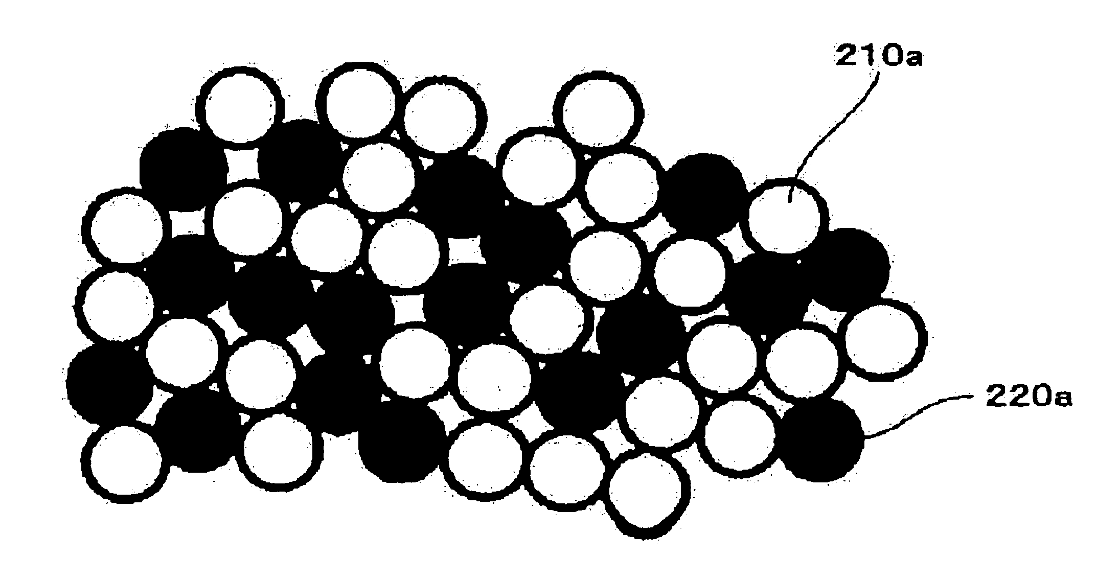
A ferroelectric memory device includes first electrodes, second electrodes arranged in a direction which intersects the first electrodes, and ferroelectric films disposed in at least intersecting regions of the first electrodes and the second electrodes. Capacitors formed of the first electrodes, the ferroelectric films, and the second electrodes are disposed in a matrix. A ferroelectric phase and a paraelectric phase are mixed in each of the ferroelectric films.

Description

CROSS REFERENCE TO THE RELATED APPLICATIONS[0001]This application is a continuation of International Patent Application No. PCT / JP02 / 09032, having an international filing date of Sep. 5, 2002 which designated the United States, the entirety of which is incorporated herein by reference. Japanese Patent Application No. 2001-269542 filed on Sep. 5, 2001 is also incorporated herein by reference in its entirety.BACKGROUND OF THE INVENTION[0002]The present invention relates to a ferroelectric memory device formed by using ferroelectric capacitors. More particularly, the present invention relates to a simple matrix type ferroelectric memory device having no cell transistor and including memory cells formed only by ferroelectric capacitors, and a method for manufacturing the same.[0003]In recent years, research and development of thin films such as PZT and SBT, ferroelectric capacitors using these thin films, ferroelectric memory devices, and the like have been extensively conducted. The st...

Claims


Application Information

Patent Timeline
Patent Type & Authority Patents(United States)
IPC IPC(8): H01L27/115H01L21/70H01L21/8246H01L21/02H10B20/00H10B69/00
CPCH01L27/11502H01L27/11507H01L28/55H10B53/30H10B53/00
Inventor NATORI, EIJIKIJIMA, TAKESHI
Owner SEIKO EPSON CORP
Learn More