Organic EL image display device

an image display device and organic technology, applied in the direction of optical elements, identification means, instruments, etc., can solve the problems of image blurring, and achieve the effects of reducing image blurring, high brightness, and reducing image blurring

Active Publication Date: 2021-05-04
FUJIFILM CORP
View PDF12 Cites 0 Cited by
  • Summary
  • Abstract
  • Description
  • Claims
  • Application Information

AI Technical Summary

Benefits of technology

[0007]The present invention is made to solve the above problems and an object thereof is to provide an organic EL image display device with high brightness and little image blurring.
[0008]The present inventors considered that the blurring occurs based on light which travels from the inside of an organic electroluminescent layer diagonally to a circularly polarizing plate direction and carried out intensive studies in order to solve the above problems. As a result, the present inventors found that a region corresponding a region between organic electroluminescent layers is allowed to have the visible light transmittance to reduce the blurring, and the present invention has been achieved on the basis of the knowledge.
[0021]According to the present invention, it is possible to provide an organic EL image display device with high brightness and little blurring.

Problems solved by technology

On the other hand, in a case where the cholesteric liquid crystal layer is arranged without providing a light shielding layer, there is a problem that blurring in an image may be observed.

Method used


Image

  • Organic EL image display device
  • Organic EL image display device
  • Organic EL image display device

Examples


example 1

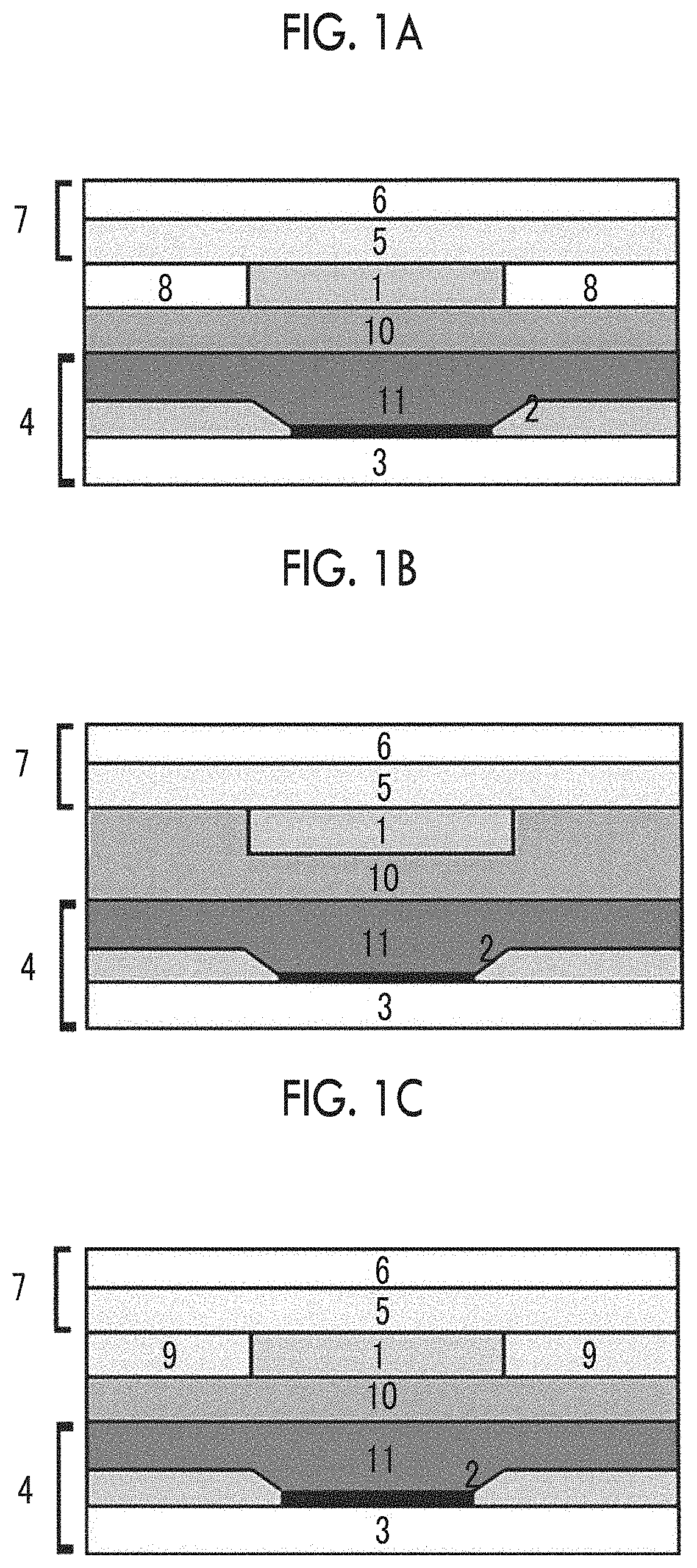
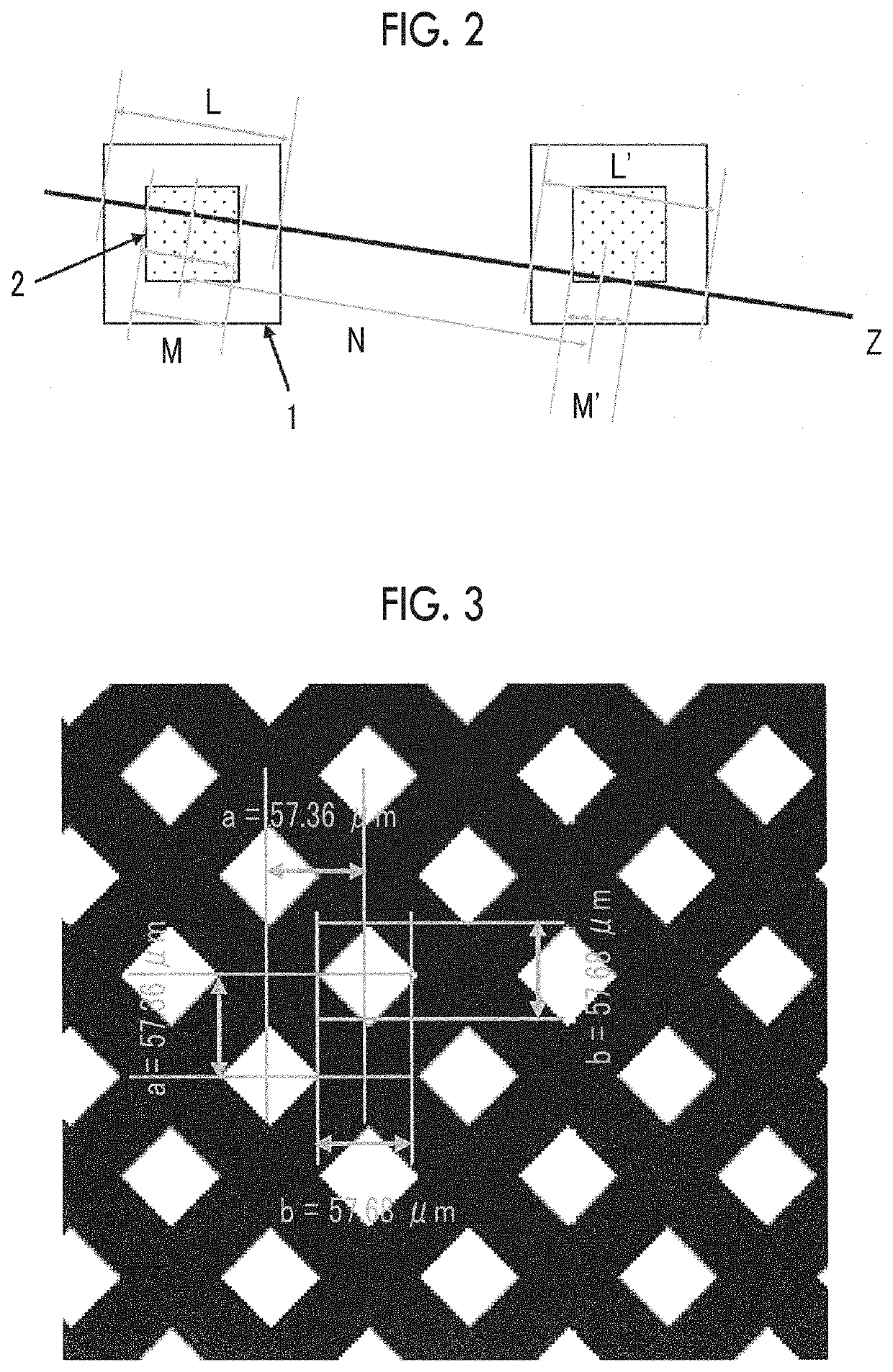
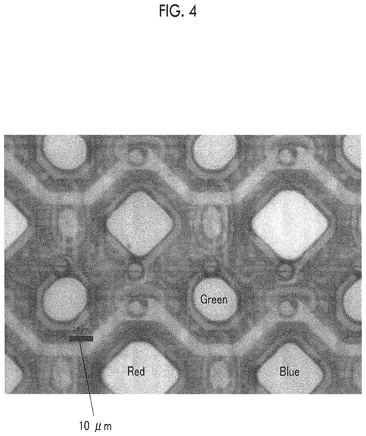
[0239]The alignment film composition A was uniformly applied to a glass substrate using a slit coater, and then dried for 2 minutes in an oven at 100° C. to obtain a glass substrate with an alignment film having a thickness of 0.5 μm. The alignment film was rubbed in a direction parallel to the coating direction. The liquid crystal composition LC-1 was applied to the rubbed surface. Next, the composition was heated and aged at a film surface temperature of 95° C. for 60 seconds, and immediately thereafter, the composition was exposed via a photo mask A shown in FIG. 3 (value of b: 57.7 μm: value of b corresponding to L of Expression (1)) at an exposure dose of 100 mJ / cm2 using a PLA-501F exposure machine (super high pressure mercury lamp) manufactured by Canon Inc. under air at 25° C. In FIG. 3, white refers to a transmission part and black refers to a shielding part. Then, by exposing the entire substrate to light under nitrogen by an air-cooled metal halide lamp (manufactured by E...

example 2

[0242]A layer having the cholesteric liquid crystal layer pattern was prepared in the same manner as in Example 1 except that a photo mask B, in which the value of b in FIG. 3 was set to 30.00 μm, was used during pattern formation. Furthermore, a layer having the cholesteric liquid crystal layer pattern and a circularly polarizing plate CP1 are laminated in the same manner as in Example 1 on the barrier layer surface of the light emitting element substrate prepared in the same manner as in Example 1 to prepare the image display device for evaluation.

example 3

[0243]A layer having the cholesteric liquid crystal layer pattern was prepared in the same manner as in Example 1 except that a photo mask C, in which the value of b in FIG. 3 was set to 20.00 μm, was used during pattern formation. Furthermore, a layer having the cholesteric liquid crystal layer pattern and a circularly polarizing plate CP1 were laminated in the same order as in Example 1 on the barrier layer surface of the light emitting element substrate prepared in the same manner as in Example 1 to prepare the image display device for evaluation.


PUM

PropertyMeasurementUnit
angleaaaaaaaaaa
angleaaaaaaaaaa
angleaaaaaaaaaa

Abstract

An organic EL image display device that includes a light emitting element substrate; and a circularly polarizing plate. The light emitting element substrate includes a reflecting layer and an organic electroluminescent layer group arranged in a matrix form on the reflecting layer. The reflecting layer, the organic electroluminescent layer group, and the circularly polarizing plate are arranged in this order. A polarization separation layer is provided between the organic electroluminescent layer group and the circularly polarizing plate, and includes polarization separation sites arranged in a matrix form corresponding to the organic electroluminescent layer group. The polarization separation site reflects light of one polarization state and transmits light of the other polarization state in light emitted from the corresponding organic electroluminescent layer. The polarization separation site is divided by a visible light transmission region. The organic EL image display device of the present invention has high brightness and little blurring.

Description

CROSS-REFERENCE TO RELATED APPLICATIONS[0001]This application is a continuation of PCT International Application No. PCT / JP2018 / 013070 filed on Mar. 29, 2018, which was published under PCT Article 21(2) in Japanese, and which claims priority under 35 U.S.C § 119 (a) to Japanese Patent Application No. 2017-068201 filed on Mar. 30, 2017, the entire content of all of which are incorporated herein by reference in their entirety.BACKGROUND OF THE INVENTION1. Field of the Invention[0002]The present invention relates to an organic EL image display device.2. Description of the Related Art[0003]In an organic electroluminescent image display device (organic EL image display device, hereinafter, simply referred to as “image display device”) that forms an image based on the light emitted from an organic electroluminescent layer, generally, a circularly polarizing plate constituted of a phase difference layer and a polarization layer is arranged in order to reduce the reflected glare of external...

Claims


Application Information

Patent Timeline
Patent Type & Authority Patents(United States)
IPC IPC(8): H01L51/52H01L27/32
CPCH01L51/5284H01L51/5271H01L27/3211H05B33/02G09F9/00G09F9/30G02B27/285H10K59/00H10K59/35H10K71/166H10K50/86H10K2102/3026H10K50/865H10K50/856
Inventor MURAMATSU, AYAKOKASHIWAGI, DAISUKEYOSHINARI, SHINICHIGOTO, RYOJI
Owner FUJIFILM CORP
Why Eureka
Try Eureka