Semiconductor device and wireless communication apparatus

a wireless communication and semiconductor technology, applied in the direction of pulse automatic control, oscillation generator, resonance circuit tuning, etc., can solve the problems of increasing and achieve the effect of maintaining manual operability and suppressing manufacturing cost and power consumption

Active Publication Date: 2021-06-15
SONY SEMICON SOLUTIONS CORP
View PDF12 Cites 0 Cited by
  • Summary
  • Abstract
  • Description
  • Claims
  • Application Information

AI Technical Summary

Benefits of technology

[0011]According to the present disclosure as described above, it is possible to provide a semiconductor device and a wireless communication apparatus each of which makes it possible to suppress the manufacturing cost and the power consumption while maintaining the manual operability.
[0012]It is to be noted that the above-described effects are not necessarily limitative. Any of the effects indicated in this description or other effects that may be understood from this description may be exerted in addition to the above-described effects or in place of the above-described effects.

Problems solved by technology

This increases the manufacturing cost, and further leads to increase in the power consumption.

Method used


Image

  • Semiconductor device and wireless communication apparatus
  • Semiconductor device and wireless communication apparatus
  • Semiconductor device and wireless communication apparatus

Examples


first embodiment

2. First Embodiment

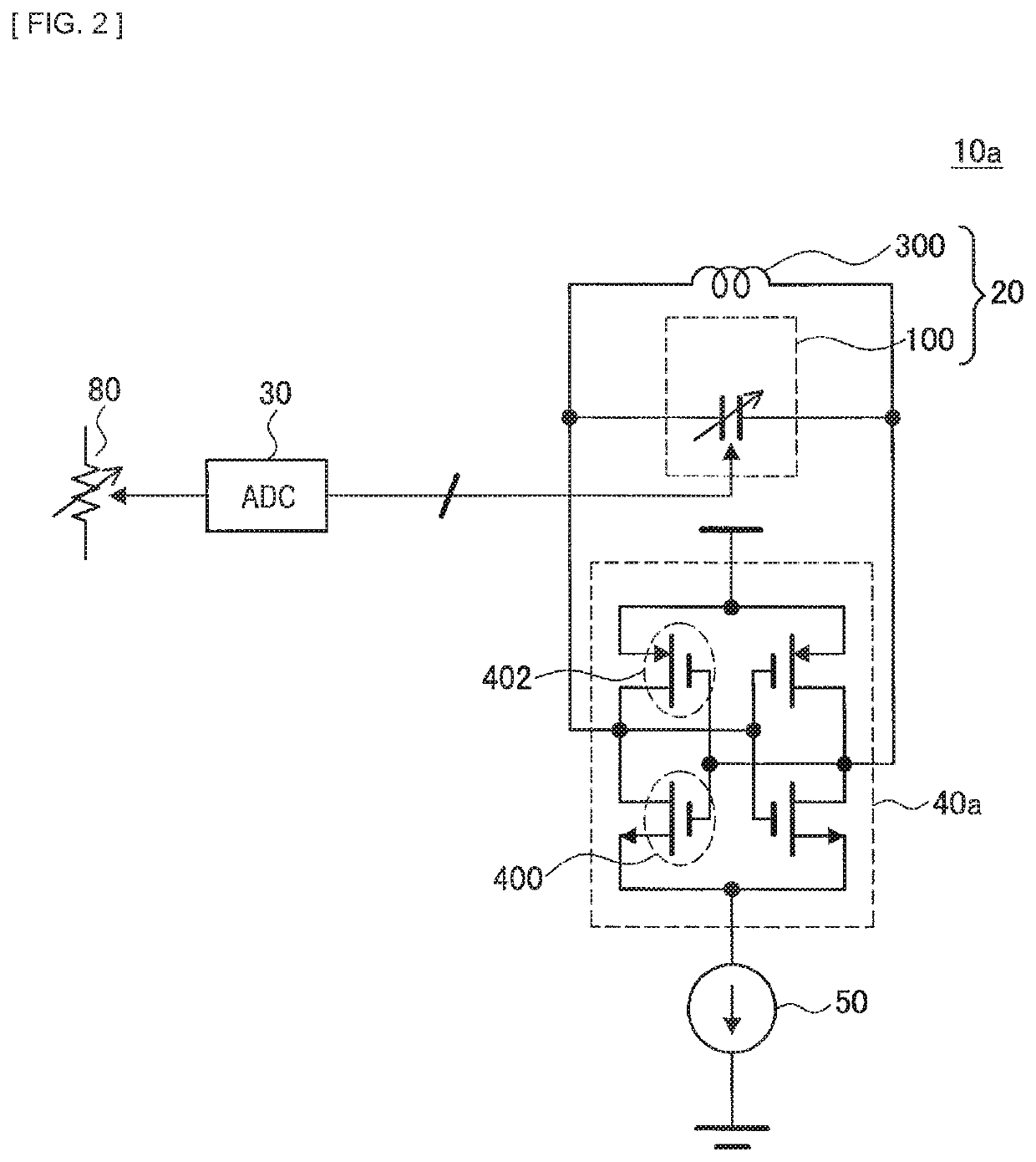
[0072]First, a first embodiment of the present disclosure is described in detail with reference to FIGS. 1 and 2. FIG. 1 is a circuit diagram schematically illustrating a configuration of an oscillator 10 according to a first embodiment of the present disclosure, and FIG. 2 is a circuit diagram schematically illustrating a configuration of an oscillator 10a according to a modification example of the present embodiment.

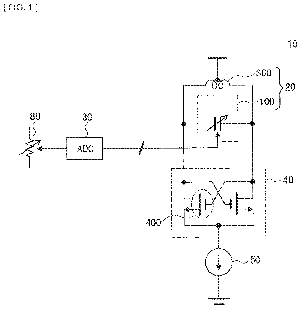
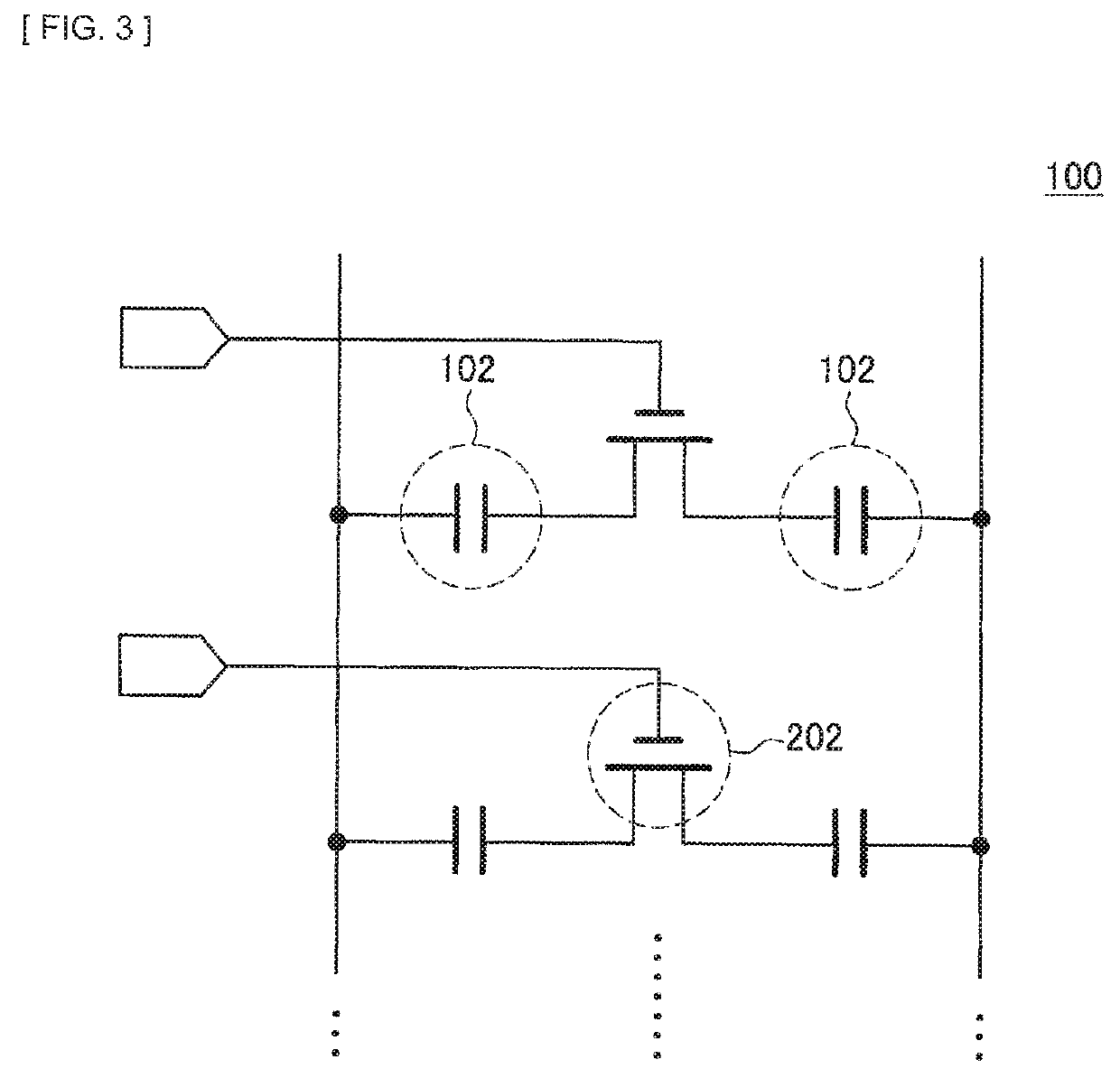
[0073]As illustrated in FIG. 1, the oscillator 10 according to the present embodiment includes an LC oscillator (oscillation circuit) 20 including a capacity bank (capacitor) 100 and the inductor 300, an AD converter (Analog Digital Converter) (conversion circuit) (that is referred to as “ADC” in the diagram) 30, a negative resistance circuit 40, and a constant current source 50. The capacity bank (capacitor) 100 includes a plurality of capacitors (small capacitors) 102 (see FIG. 3). The oscillator 10 is an oscillator that oscillates an oscillation s...

second embodiment

3. Second Embodiment

[0083]As described above, in the above-described first embodiment of the present disclosure, appropriately selecting the capacity values of the respective capacitors 102 included in the capacity bank 100 and the number of capacitors 102 included in the capacity bank 100 makes it possible to generate an oscillation signal whose oscillation frequency linearly and continuously varies with respect to an inputted digital signal. In the first embodiment, however, the frequency of an oscillation signal is varied by discretely switching the total capacity value of the capacity bank 100 with a digital signal. In fact, the oscillator 10 thus has to switch the total capacity value of the capacity bank 100 within a minute variation range to generate an oscillation signal whose oscillation frequency linearly and continuously varies with respect to a digital signal as illustrated in FIG. 4.

[0084]In a semiconductor manufacturing process, however, the minimum capacity value or c...

embodiment 1

3.2 Present Embodiment 1

[0092]Accordingly, the method of controlling the frequency of the oscillator 10 is proposed in the second embodiment of the present disclosure. The method of controlling the frequency of the oscillator 10 makes it possible to generate an oscillation signal whose oscillation frequency linearly and continuously varies with respect to a digital signal within a minute variation range even if the manufacturable minimum capacity value is limited by the semiconductor manufacturing process to be used. The following describes the present embodiment with reference to FIGS. 5 to 9. Each of FIGS. 5 to 7 is an explanatory diagram for describing a method of controlling a frequency according to a second embodiment of the present disclosure. In addition, FIG. 8 is an explanatory diagram describing an example of variations in a capacity value in the method of controlling the frequency according to the present embodiment. FIG. 9 is an explanatory diagram describing an example ...


PUM


Abstract

There is provided a semiconductor device including an oscillation circuit that includes a plurality of capacitors provided on a semiconductor substrate, a conversion circuit that converts an analog signal into a digital signal, and a switch circuit that switches the capacitors on the basis of the digital signal. Further, an oscillation frequency linearly varies with respect to a variation in the analog signal.

Description

CROSS REFERENCE TO RELATED APPLICATIONS[0001]This application is a U.S. National Phase of International Patent Application No. PCT / JP2018 / 032801 filed on Sep. 5, 2018, which claims priority benefit of Japanese Patent Application No. JP 2017-236992 filed in the Japan Patent Office on Dec. 11, 2017. Each of the above-referenced applications is hereby incorporated herein by reference in its entirety.TECHNICAL FIELD[0002]The present disclosure relates to a semiconductor device and a wireless communication apparatus.BACKGROUND ART[0003]A radio receiver is able to obtain a sound signal by amplifying a high-frequency radio signal with an RF (Radio Frequency) amplifier, converting the amplified radio signal into an IF (Intermediate Frequency) signal having a low frequency with a mixer circuit, and performing demodulation with a demodulator by using the converted IF signal. It is possible to perform frequency conversion for converting a high-frequency radio signal into an IF signal by multip...

Claims


Application Information

Patent Timeline
Patent Type & Authority Patents(United States)
IPC IPC(8): H03B5/12H03L7/099
CPCH03B5/1265H03L7/0992H03B5/1215H03B5/1228H03J5/0254H03J2200/10
Inventor TAKEUCHI, HIDENORIOKANOBU, TAIWAARISAKA, NAOYATOMIYAMA, HITOSHI
Owner SONY SEMICON SOLUTIONS CORP
Why Eureka
Try Eureka