Check patentability & draft patents in minutes with Patsnap Eureka AI!

Three dimensional semiconductor memory devices

a semiconductor memory and three-dimensional technology, applied in semiconductor devices, instruments, electrical equipment, etc., can solve the problems of high equipment requirements, limited integration density of 2d or planar semiconductor devices,

Active Publication Date: 2021-09-21
SAMSUNG ELECTRONICS CO LTD
View PDF13 Cites 0 Cited by
  • Summary
  • Abstract
  • Description
  • Claims
  • Application Information

AI Technical Summary

Benefits of technology

The patent text describes three dimensional semiconductor devices with memory cells that have a unique configuration to improve their performance. The devices include conductive lines and first and second variable resistance patterns that are arranged in a cross-point configuration with the second conductive lines. The memory cells also have a unique design with a sidewall portion and horizontal portions in the cross-direction of the first conductive lines. The technical effect of this design is to enhance the read and write performance of the memory cells. Additionally, the patent describes different layouts for the conductive lines and memory cells on the substrate, which further improve the performance of the semiconductor devices.

Problems solved by technology

However, a high-cost equipment is required for such a fine pattern formation in a 2D or planar semiconductor manufacturing process and increase of the integration density of the 2D or planar semiconductor device is limited.

Method used


Image

  • Three dimensional semiconductor memory devices
  • Three dimensional semiconductor memory devices
  • Three dimensional semiconductor memory devices

Examples


Embodiment Construction

[0023]Various example embodiments will now be described more fully hereinafter with reference to the accompanying drawings. Like reference numerals may refer to like elements throughout this application.

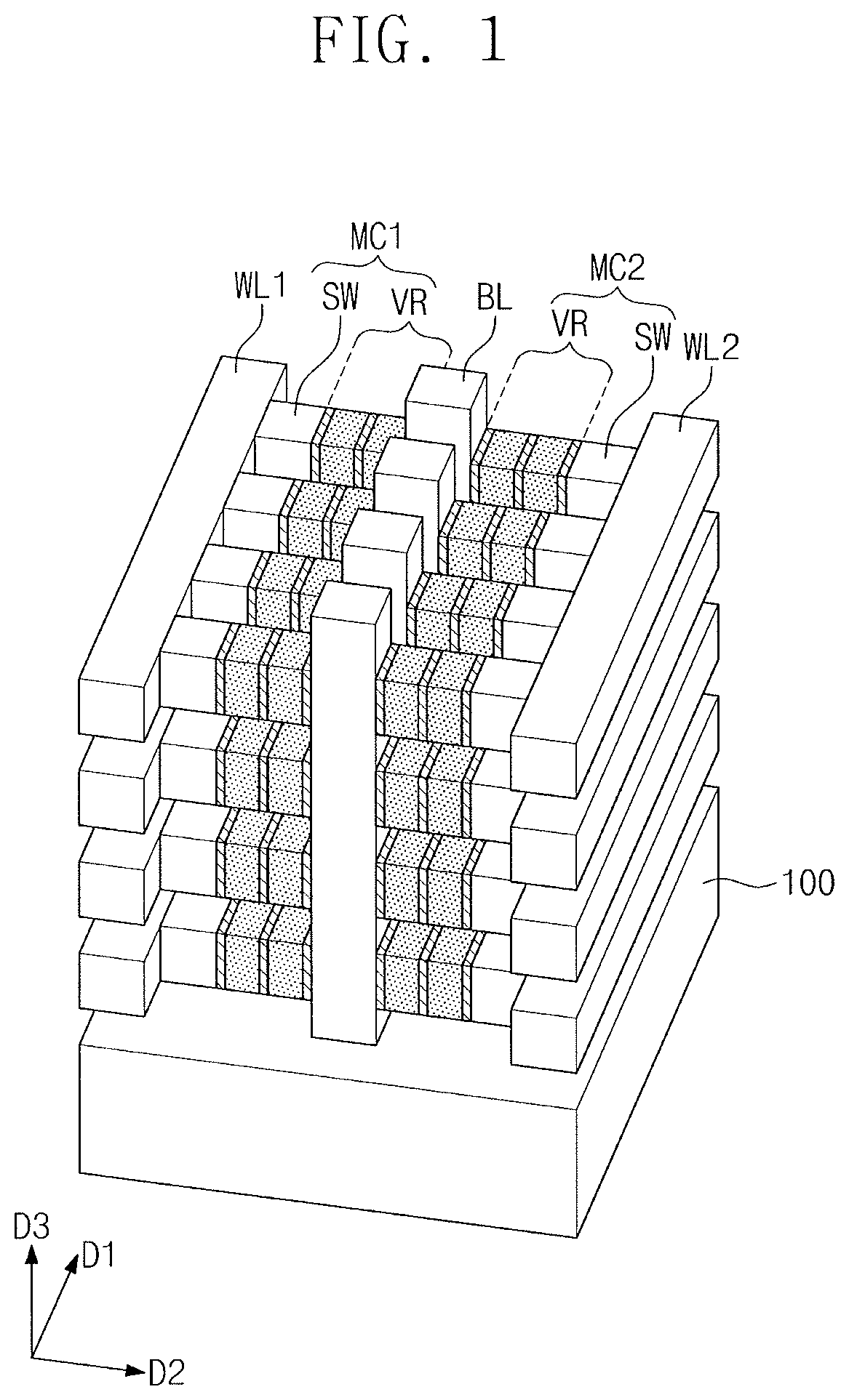
[0024]FIG. 1 is a schematic perspective view illustrating a three-dimensional semiconductor memory device according to example embodiments.

[0025]Referring to FIG. 1, a three-dimensional (3D) semiconductor memory device may include a cross point memory cell array including memory cells MC1 and MC2 that are three dimensionally arranged on a substrate 100. The cross-point memory cell array may include word lines WL1 and WL2, bit lines BL crossing the word lines WL1 and WL2, and the memory cells MC1 and MC2 arranged at cross points between the word lines WL1 and WL2 and the bit lines BL.

[0026]The word lines WL1 and WL2 may include first word lines WL1 at first sides of the bit lines BL and second word lines WL2 at second sides of the bit lines BL opposite to the first sides of the bit li...


PUM

PropertyMeasurementUnit
phase transition temperatureaaaaaaaaaa

Abstract

A three-dimensional semiconductor memory device includes first conductive lines extending horizontally in a first direction, a second conductive line extending vertically in a second direction perpendicular to the first direction, and memory cells at cross-points between the first conductive lines and the second conductive line. The first conductive lines are laterally spaced apart from each other in a third direction crossing the first direction. Each of the memory cells includes a variable resistance element and a switching element that are horizontally arranged. The variable resistance element includes a first variable resistance pattern and a second variable resistance pattern arranged in the second direction, a first electrode between the first variable resistance pattern and the first conductive line, a second electrode between the second variable resistance pattern and the second conductive line, and a third electrode between the first variable resistance pattern and the second variable resistance pattern.

Description

CROSS-REFERENCE TO RELATED APPLICATION[0001]Korean Patent Application No. 10-2019-0069618, filed on Jun. 12, 2019, in the Korean Intellectual Property Office, and entitled: “Three Dimensional Semiconductor Memory Devices,” is incorporated by reference herein in its entirety.BACKGROUND1. Field[0002]Example embodiments of the present disclosure relate to three-dimensional semiconductor memory devices, and more specifically, to three-dimensional semiconductor memory devices including variable resistance memory cells.2. Description of the Related Art[0003]A semiconductor device is highly integrated to meet demands of high performance and low costs. For example, an integration degree of a two-dimensional (2D) or planar semiconductor device is mainly determined by an area used for a unit memory cell. Therefore, the integration density of the 2D or planar semiconductor device depends on a technique used for a fine pattern formation. However, a high-cost equipment is required for such a fin...

Claims


Application Information

Patent Timeline
Patent Type & Authority Patents(United States)
IPC IPC(8): H01L27/24H01L45/00G11C5/06
CPCH01L27/249G11C5/063H01L45/06H01L45/1253H01L45/141H10B63/00H10B63/845H10N70/841H10N70/882H10N70/231H01L29/861H10B63/20H10N70/20
Inventor SONG, SI-HOPARK, JEONGHEECHO, CHANGHYUN
Owner SAMSUNG ELECTRONICS CO LTD
Features
  • R&D
  • Intellectual Property
  • Life Sciences
  • Materials
  • Tech Scout
  • Unparalleled Data Quality
  • Higher Quality Content
  • 60% Fewer Hallucinations
Learn More