Supercharge Your Innovation With Domain-Expert AI Agents!

Light emitting diode with ion implanted resistive area, manufacturing method of light emitting diode with ion implanted resistive area and display device including light emitting diode with ion implanted resistive area

a technology of light emitting diodes and manufacturing methods, applied in the direction of basic electric elements, semiconductor devices, electrical apparatus, etc., can solve the problems of reducing light emitting efficiency, reducing light extraction efficiency (lee), and limiting the efficiency of the formation process of the electrode layer and the transfer process. achieve the effect of high efficiency

Active Publication Date: 2021-09-28
SAMSUNG ELECTRONICS CO LTD
View PDF34 Cites 0 Cited by
  • Summary
  • Abstract
  • Description
  • Claims
  • Application Information

AI Technical Summary

Benefits of technology

[0009]The present disclosure provides a flip-chip LED with high efficiency including a current confinement structure and a manufacturing method thereof, and a display device including such an LED.
[0010]According to an aspect of the disclosure, flip-chip light-emitting diode (LED) may include a light-emitting layer; an n-type semiconductor layer disposed on an upper surface of the light-emitting layer; a p-type semiconductor layer disposed on a lower surface of the light-emitting layer; an n-electrode connected to the n-type semiconductor layer; a p-electrode connected to the p-type semiconductor layer; a passivation layer disposed on sidewalls of the LED and a surface on an opposite side of a light-emitting surface of the LED; a reflective layer disposed on the passivation layer, and that reflects light emitted from the light-emitting layer; and a resistive area disposed on side surfaces of the light-emitting layer, and that restricts current flow from the light-emitting layer to the sidewalls.

Problems solved by technology

However, in the case of an LED in a vertical type, an electrode is arranged on a light-emitting surface of an LED, and thus there is a limitation that the light extraction efficiency (LEE) decreases accordingly, and the light emitting efficiency is reduced.
In addition, in the case of an LED in a vertical type, there is also a limitation in terms of efficiency of a formation process of an electrode layer and a transferring process of forming an electronic connection part.

Method used


Image

  • Light emitting diode with ion implanted resistive area, manufacturing method of light emitting diode with ion implanted resistive area and display device including light emitting diode with ion implanted resistive area
  • Light emitting diode with ion implanted resistive area, manufacturing method of light emitting diode with ion implanted resistive area and display device including light emitting diode with ion implanted resistive area
  • Light emitting diode with ion implanted resistive area, manufacturing method of light emitting diode with ion implanted resistive area and display device including light emitting diode with ion implanted resistive area

Examples


Embodiment Construction

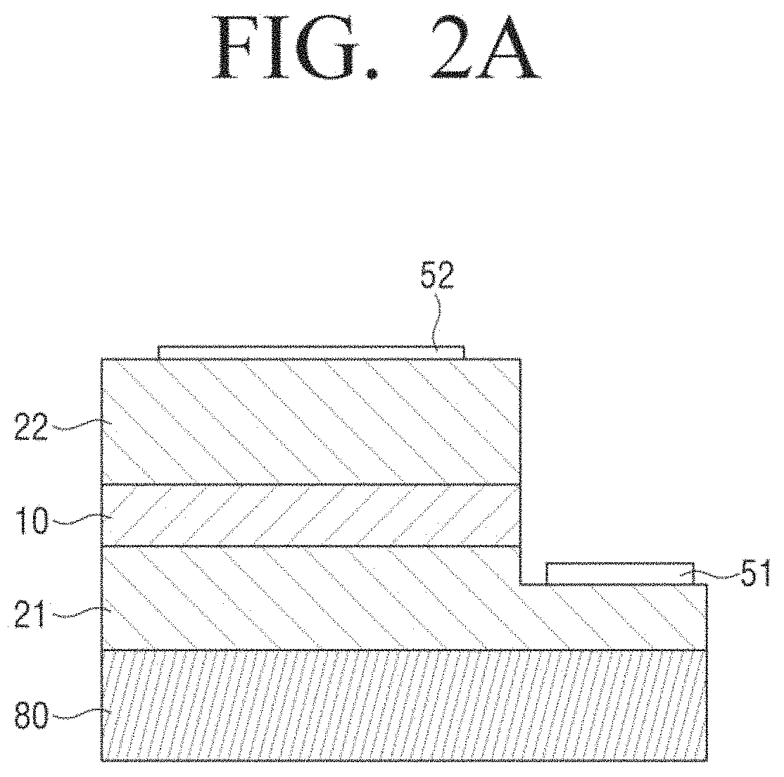
[0037]Various modifications may be made to the embodiments of the disclosure, and there may be various types of embodiments. Accordingly, specific embodiments will be illustrated in drawings, and the embodiments will be described in detail in the detailed description. However, it should be noted that the various embodiments do not limit the scope of the disclosure to a specific embodiment, and that they should be interpreted to include various modifications, equivalents, and / or alternatives of the embodiments of the disclosure. Also, with respect to the detailed description of the drawings, similar components may be designated by similar reference numerals.

[0038]Meanwhile, in explaining the disclosure, in case it is determined that detailed explanation of related known functions or features may unnecessarily confuse the gist of the disclosure, the detailed explanation may be omitted.

[0039]In addition, the embodiments below may be modified in various different forms, and the scope of...


PUM

PropertyMeasurementUnit
areaaaaaaaaaaa
light wavelengthaaaaaaaaaa

Abstract

An LED, a manufacturing method thereof, and a display device including an LED are provided. Specifically, the disclosure relates to a flip-chip LED with high efficiency including a current confinement structure and a manufacturing method thereof, and a display device including such an LED. In particular, a flip-chip LED according to the disclosure includes a resistive area that surrounds a light-emitting layer and restricts current flow from the light emitting layer to the sidewalls.

Description

CROSS-REFERENCE TO RELATED APPLICATION(S)[0001]This application is based on and claims priority under 35 U.S.C. § 119 to Korean Patent Application No. 10-2018-0141291, filed on Nov. 16, 2018, in the Korean Intellectual Property Office, the disclosure of which is incorporated by reference herein in its entirety.BACKGROUND1. Field[0002]The disclosure relates to a light-emitting diode (LED), a manufacturing method thereof, and a display device including an LED, and more particularly, to a flip-chip LED having a current confinement structure and a manufacturing method thereof, and a display device including such an LED.2. Description of Related Art[0003]LEDs are being applied to various industrial fields based on the relatively high light-emitting efficiency and long lifespan of LEDs. In particular, LEDs are being commercialized in the field of displays, as well as in the field of general lighting.[0004]Meanwhile, in particular, following the trend of high performance and high efficienc...

Claims


Application Information

Patent Timeline
Patent Type & Authority Patents(United States)
IPC IPC(8): H01L33/00H01L31/12H01L29/26H01L27/15H01L33/10H01L33/62H01L25/075
CPCH01L33/0095H01L25/0753H01L33/10H01L33/62H01L2933/0066H01L33/60H01L33/486H01L33/46H01L2933/0025H01L2933/0058H01L2933/0016H01L33/36H01L33/14H01L25/167H01L33/025H01L33/24H01L33/145H01L33/0008H01L33/005H01L27/156
Inventor OTA, JITSUOKANG, JIHOONKIM, SUNGTAEKIMURA, SHUNSUKECHA, YONGDOK
Owner SAMSUNG ELECTRONICS CO LTD
Features
  • R&D
  • Intellectual Property
  • Life Sciences
  • Materials
  • Tech Scout
  • Unparalleled Data Quality
  • Higher Quality Content
  • 60% Fewer Hallucinations
Learn More