
Semiconductor package having multi-level and multi-directional shape narrowing vias

a technology of multi-level and multi-directional shape, applied in the field of semiconductor package, can solve the problems of difficult handling and testing of solder balls, difficulty in attaching a desired number of solder balls, and difficulty in mounting a large number of boards, and achieve the effect of reducing undulation and high reliability

Active Publication Date: 2021-11-16
SAMSUNG ELECTRONICS CO LTD
View PDF32 Cites 0 Cited by
  • Summary
  • Abstract
  • Description
  • Claims
  • Application Information

AI Technical Summary

Benefits of technology

[0006]An aspect of the present inventive concept may be to provide a semiconductor package with high reliability by reducing undulations caused in a redistribution substrate having a redistribution layer.

Problems solved by technology

However, as semiconductor chips become smaller, it becomes difficult to attach a desired number of solder balls, and handling and testing of the solder balls becomes difficult.
In addition, there may be a problem in that the number of boards to be mounted depends on the size of the semiconductor chip.

Method used


Image

  • Semiconductor package having multi-level and multi-directional shape narrowing vias
  • Semiconductor package having multi-level and multi-directional shape narrowing vias
  • Semiconductor package having multi-level and multi-directional shape narrowing vias

Examples


Embodiment Construction

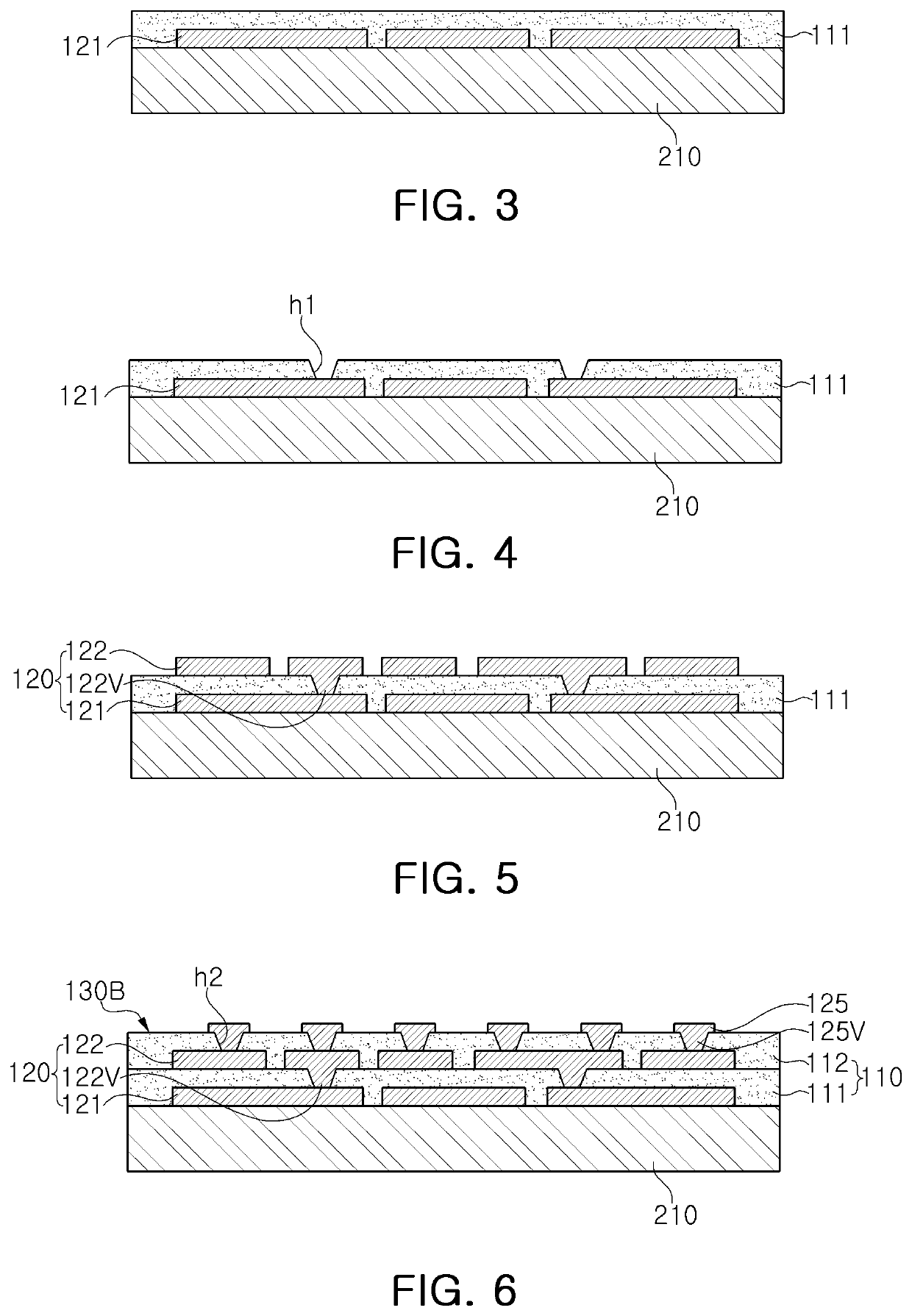
[0018]Hereinafter, various embodiments of the present inventive concept will be described with reference to the accompanying drawings.

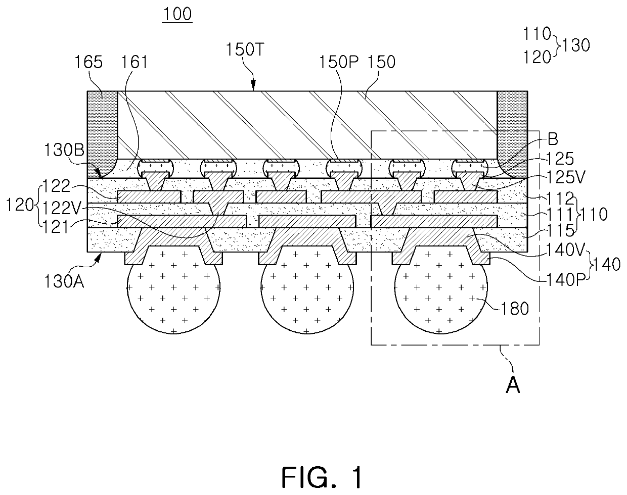
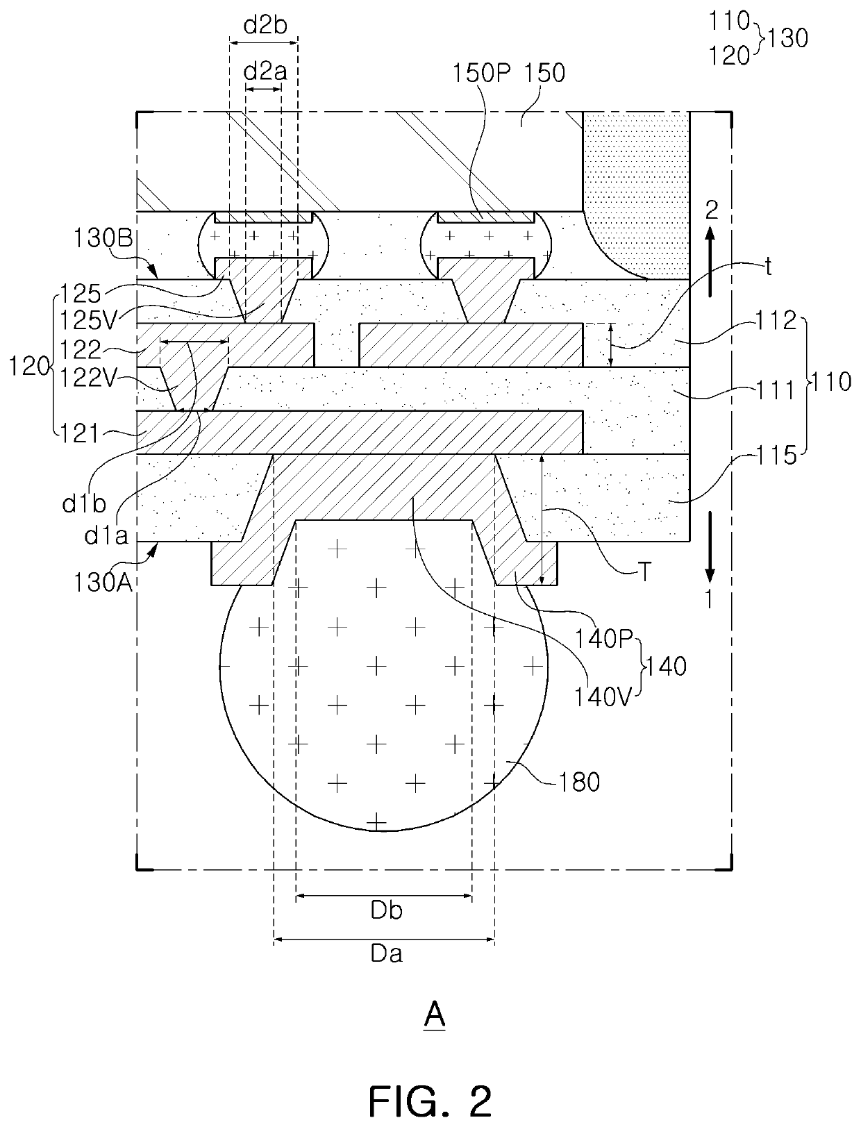
[0019]FIG. 1 is a cross-sectional view illustrating a semiconductor package according to an example embodiment, and FIG. 2 is an enlarged cross-sectional view illustrating portion “A” of the semiconductor package illustrated in FIG. 1.

[0020]Referring to FIG. 1, a semiconductor package 100 according to an example embodiment may be a semiconductor package in the form of a fan-out wafer level package (FOWLP). The semiconductor package 100 may include a redistribution substrate 130 having a first surface 130A and a second surface 130B disposed opposite each other and facing away from one another. The semiconductor package 100 may further include under bump metallurgy (UBM) layers 140 disposed on the first surface 130A of the redistribution substrate 130, and a semiconductor chip 150 disposed on the second surface 130B of the redistribution substrate 130.

[...


PUM

PropertyMeasurementUnit
thicknessaaaaaaaaaa
areaaaaaaaaaaa
thicknessaaaaaaaaaa

Abstract

A semiconductor package includes a redistribution substrate having first and second surfaces opposed to each other, and including an insulation member, a plurality of redistribution layers on different levels in the insulation member, and a redistribution via having a shape narrowing from the second surface toward the first surface in a first direction; a plurality of UBM layers, each including a UBM pad on the first surface of the redistribution substrate, and a UBM via having a shape narrowing in a second direction, opposite to the first direction; and at least one semiconductor chip on the second surface of the redistribution substrate, and having a plurality of contact pads electrically connected to the redistribution layer adjacent to the second surface among the plurality of redistribution layers.

Description

CROSS-REFERENCE TO RELATED APPLICATION[0001]This application claims the benefit of priority under 35 U.S.C. § 119 to Korean Patent Application No. 10-2018-0164403, filed on Dec. 18, 2018, in the Korean Intellectual Property Office, the disclosure of which is incorporated herein by reference in its entirety.BACKGROUND1. Field[0002]The present inventive concept relates to a semiconductor package. More particularly, the present inventive concept relates to a semiconductor package including vias having tapered shapes.2. Description of Related Art[0003]The semiconductor package may be the result when a semiconductor chip, such as an integrated circuit, is implemented in a form suitable for use in an electronic product. As the electronics industry has developed in recent years, semiconductor packages have developed in various ways aimed at downsizing, weight saving, and manufacturing cost reductions.[0004]As a method of manufacturing a semiconductor package, there may be provided a wafer ...

Claims


Application Information

Patent Timeline
Patent Type & Authority Patents(United States)
IPC IPC(8): H01L23/49H01L23/31H01L23/36H01L23/538H01L23/498H01L23/367H01L23/00H01L21/48H01L21/56H01L23/42
CPCH01L23/49838H01L23/3128H01L23/367H01L23/49816H01L23/49822H01L23/5383H01L23/5386H01L24/08H01L21/4853H01L21/4857H01L21/568H01L23/42H01L2224/024H01L2224/0235H01L2224/02331H01L2224/02371H01L2224/08235H01L23/49827H01L21/486H01L25/18H01L2224/0231H01L2224/02333H01L2224/02381H01L2224/02379H01L2224/0401H01L2924/15311H01L2224/81005H01L2224/73204H01L2224/16227H01L2924/18161H01L2224/33181H01L2224/2919H01L2224/2929H01L2224/29299H01L2224/32225H01L2224/32245H01L2224/32013H01L24/16H01L24/13H01L24/29H01L24/32H01L24/33H01L2224/73253H01L2224/83005H01L24/83H01L24/81H01L2221/68359H01L2224/92225H01L2221/68345H01L21/6835H01L2224/131H01L2924/0665H01L2924/00014H01L2924/00012H01L2224/16225H01L2924/00H01L2924/014H01L23/525H01L23/485H01L24/06H01L23/481H01L21/0274H01L25/0657
Inventor PARK, JUNG HOKIM, JONG YOUNBAE, MIN JUN
Owner SAMSUNG ELECTRONICS CO LTD
Learn More