[0006]An object of the present invention is to overcome the defects in the current technology, and provide a large-scale silicon-based lithium niobate film electro-optic modulator array and an integration method thereof, in which the difficulty of a fabrication process of a lithium niobate crystal layer is reduced through structural design, requirements on precision of bonding lithium niobate and silicon is reduced, and fabrication and bonding of the large-scale array lithium niobate crystal layer can be completed at one time, so that production efficiency of the silicon-based lithium niobate film electro-optic modulator array is greatly improved. Through design and optimization of the structure of the silicon crystal layers, light can be naturally alternated and mutually transmitted in silicon waveguides and lithium niobate waveguides, and a high-performance electro-optic modulation effect of the lithium niobate film is achieved. In addition, according to the method of the present invention, the advantage in maturity of the standardized silicon-based integration technology is utilized, and a complex chip fabrication process is concentrated in the silicon crystal layers, so that technology errors in the chip fabrication process are reduced, and performance stability of the whole silicon-based lithium niobate film electro-optic modulator array is guaranteed.
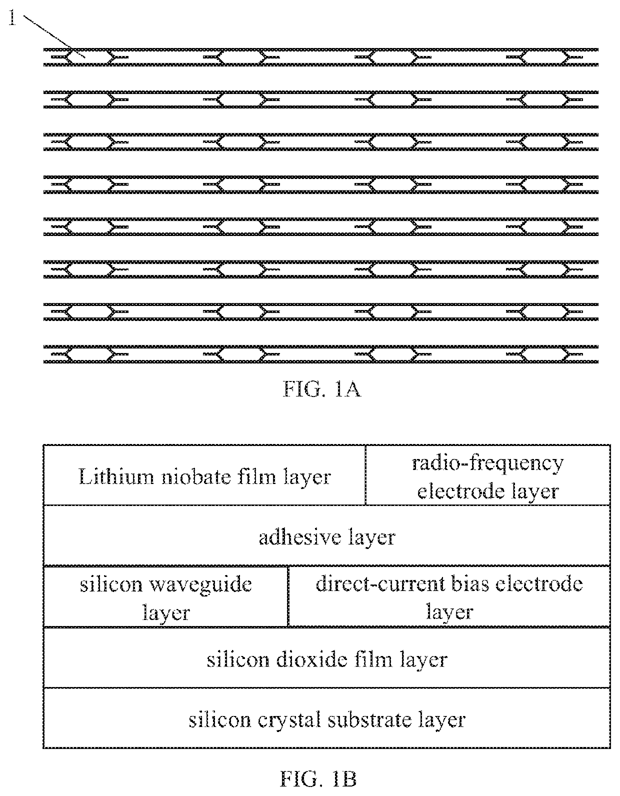
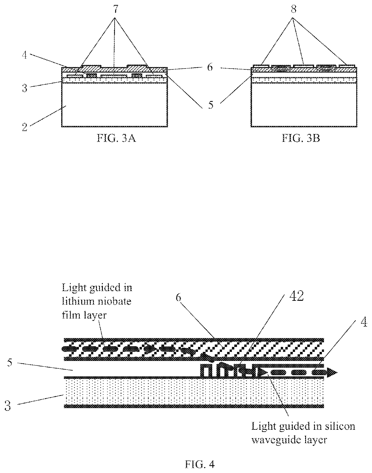
[0011]In the present invention, in one silicon-based lithium niobate film electro-optic modulator, the silicon crystal substrate layer provides a substrate material for integrating the silicon-based lithium niobate film electro-optic modulator; the silicon dioxide film layer can be formed by performing an oxidation process above the silicon crystal substrate layer, and the silicon dioxide film layer serves as a lower cladding layer for the optical waveguide and provides a binding effect on light in the waveguide; the silicon waveguide layer is formed by silicon crystal growth above the silicon dioxide film layer; a waveguide interconnection structure including optical splitters and optical couplers is formed by performing dry etching or wet etching on the silicon waveguide layer, and the silicon waveguide layer serves as a core of the optical waveguide and can provide functions of light splitting, coupling, direct-current biasing and light guiding in partial regions; the adhesive layer is located above the silicon waveguide layer and can be used for bonding the silicon waveguide layer and the lithium niobate film layer; the lithium niobate film layer is located above the adhesive layer and is a complete lithium niobate wafer subjected to etching and used for light guiding in partial regions and radio-frequency signal application. Ridge structures are formed on the lithium niobate film layer by etching and used for enhancing the binding effect on light during light guiding; a direct-current bias voltage can be applied to the direct-current bias electrode layer to generate an electric field in one section of the silicon waveguide layer so as to change an effective refractive index in the section, so that a phase change of light is caused; and a radio-frequency signal can be applied to the radio-frequency electrode layer to generate an electric field in one section of the lithium niobate film layer so as to change an effective refractive index in the section, so that a phase change of light is caused.
[0026]Compared with the current technology, the silicon-based lithium niobate film electro-optic modulator array and the integration method thereof provided by the invention have the following advantages:
[0027]1. Complex structures such as modulator interconnection, optical splitters, breakpoints and optical couplers are realized in the silicon waveguide layers, and functional effectiveness and stability of the large-scale silicon-based lithium niobate film electro-optic modulator array are guaranteed.
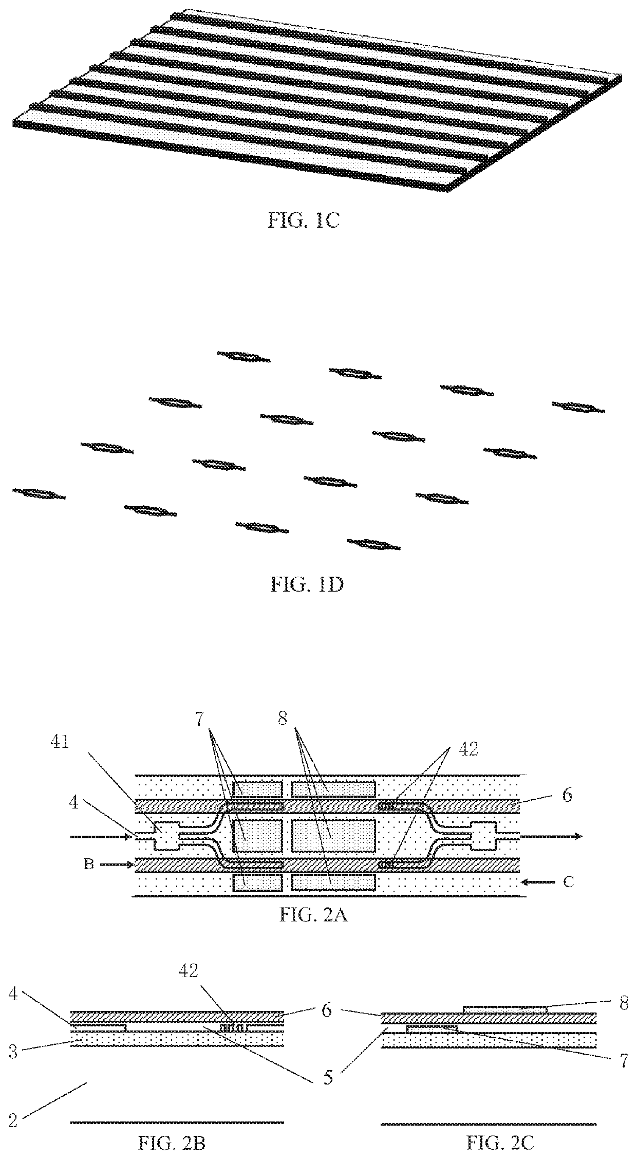
[0028]2. By virtue of the design of the periodic structure, the large-scale silicon-based lithium niobate film electro-optic modulator array can be fabricated simultaneously at one time, besides, the lithium niobate film layer does not need to be cut, and the difficulty of bonding the modulator array is as same as that of bonding a single modulator, so that the structure provided by the invention can greatly improve fabrication efficiency of the large-scale silicon-based lithium niobate film electro-optic modulator array, thereby providing strong support for complex photon signal processing systems.
[0029]3. By utilizing the silicon-based lithium niobate film electro-optic modulator integration technology, the radio-frequency signal is applied to the lithium niobate film layer, and the advantages of high electro-optic efficiency, low insertion loss and ultra-high modulation bandwidth of lithium niobate are exerted. The silicon-based lithium niobate film electro-optic modulator array and the integration method thereof can play a role in low-power consumption large-bandwidth microwave photon applications.

