Filter circuit, filter circuit element, and multi/demultiplexer

a filter circuit and filter element technology, applied in the field of filter circuits, can solve the problems of increasing insertion loss in the pass frequency band, difficult to achieve impedance matching over a wide band, etc., and achieve the effects of reducing or preventing insertion loss, increasing insertion loss in the stop frequency band, and reducing insertion loss in the pass frequency band

Active Publication Date: 2022-01-18
MURATA MFG CO LTD
View PDF12 Cites 0 Cited by
  • Summary
  • Abstract
  • Description
  • Claims
  • Application Information

AI Technical Summary

Benefits of technology

[0007]Preferred embodiments of the present invention provide filter circuits and multi / demultiplexers including the same, in each of which attenuation in a stop frequency band is increased while significantly reducing or preventing an insertion loss in a pass frequency band, or in each of which the insertion loss in the pass frequency band is reduced while ensuring the attenuation in the stop frequency band.

Problems solved by technology

In such a low pass filter, when an inductance of the inductive reactance circuit connected in series is increased in order to increase attenuation in a stop frequency band (high-frequency band), a reactance change with respect to a frequency change is increased in a pass frequency band (low-frequency band), and it becomes difficult to achieve impedance matching over a wide band.
Additionally, since the reactance is increased in the pass frequency band (low-frequency band), an insertion loss in the pass frequency band is increased.

Method used


Image

  • Filter circuit, filter circuit element, and multi/demultiplexer
  • Filter circuit, filter circuit element, and multi/demultiplexer
  • Filter circuit, filter circuit element, and multi/demultiplexer

Examples


first preferred embodiment

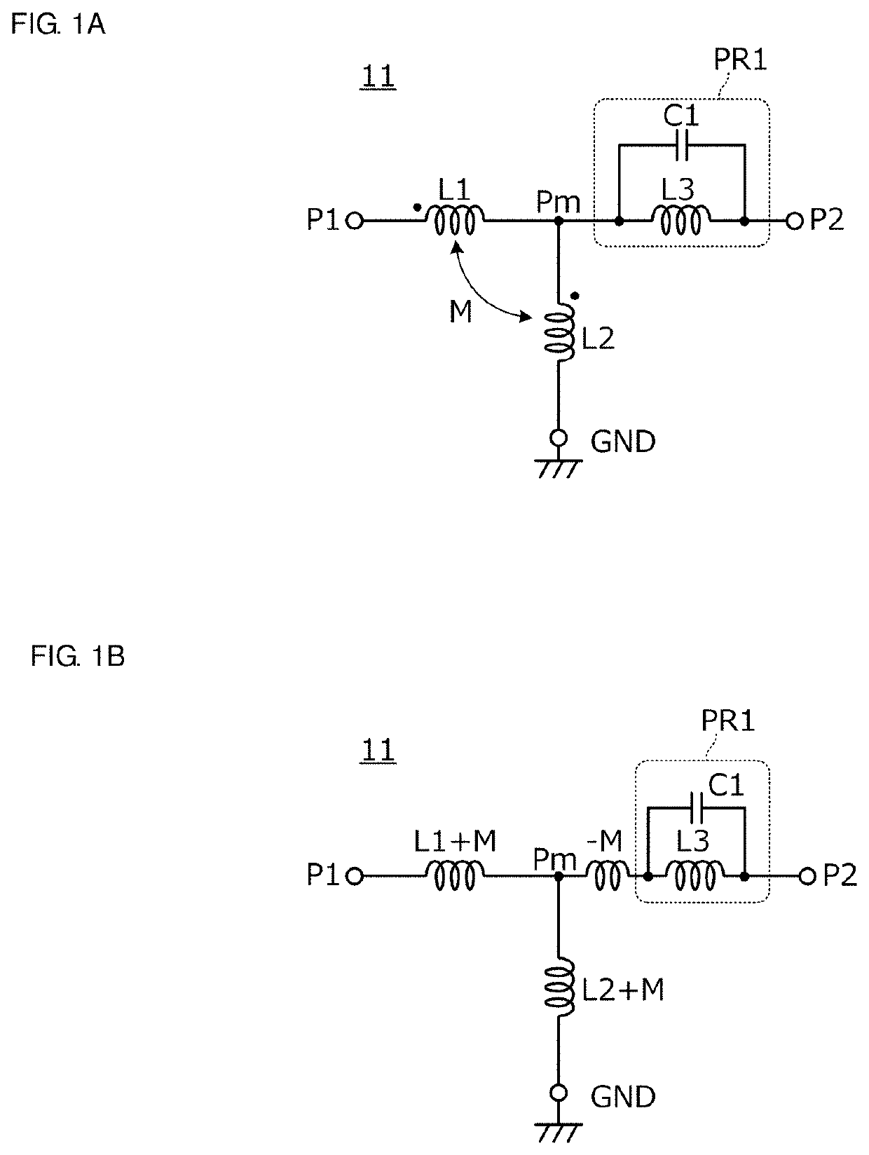
[0051]In a first preferred embodiment of the present invention, an example applied to a low pass filter will be described.

[0052]FIG. 1A is a circuit diagram of a low pass filter 11 according to the first preferred embodiment. FIG. 1B is an equivalent circuit diagram of the low pass filter 11.

[0053]The low pass filter 11 of the first preferred embodiment includes a first port P1, a second port P2, an intermediate node Pm between the first port P1 and the second port P2, and a ground terminal GND. Both the first port P1 and the second port P2 are input / output ports, and one is included in an input port, and the other is included in an output port.

[0054]Further, the low pass filter 11 includes a first inductor L1, a second inductor L2, a third inductor L3, and a first capacitor C1.

[0055]The first inductor L1 is electrically connected between the first port P1 and the intermediate node Pm. The second inductor L2 is electrically connected between the intermediate node Pm and the ground t...

second preferred embodiment

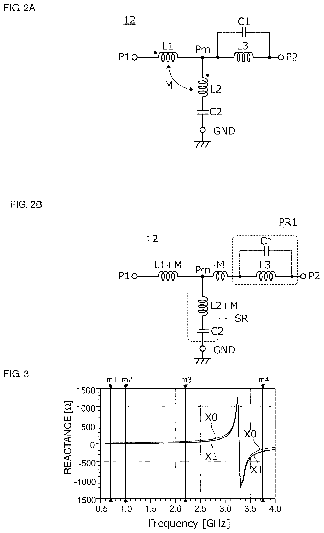
[0063]In a second preferred embodiment of the present invention, also, an example applied to a low pass filter will be described.

[0064]FIG. 2A is a circuit diagram of a low pass filter 12 according to the second preferred embodiment. FIG. 2B is an equivalent circuit diagram of the low pass filter 12.

[0065]The low pass filter 12 of the second preferred embodiment includes a first port P1, a second port P2, an intermediate node Pm between the first port P1 and the second port P2, and a ground terminal GND. Both the first port P1 and the second port P2 are input / output ports, and one is included in an input port, and the other is included in an output port.

[0066]Further, the low pass filter 12 includes a first inductor L1, a second inductor L2, a third inductor L3, a first capacitor C1, and a second capacitor C2.

[0067]The first inductor L1 is electrically connected between the first port P1 and the intermediate node Pm. The second inductor L2 is electrically connected between the inter...

third preferred embodiment

[0113]In a third preferred embodiment of the present invention, an example applied to a high pass filter will be described.

[0114]FIG. 5A is a circuit diagram of a high pass filter 13 according to the third preferred embodiment. FIG. 5B is an equivalent circuit diagram of the high pass filter 13.

[0115]The high pass filter 13 of the third preferred embodiment includes a first port P1, a second port P2, an intermediate node Pm between the first port P1 and the second port P2, and a ground terminal GND. Both the first port P1 and the second port P2 are input / output ports, and one is included in an input port, and the other is included in an output port.

[0116]Further, the high pass filter 13 includes a first inductor L1, a second inductor L2, a third inductor L3, and a third capacitor C3.

[0117]The first inductor L1 is electrically connected between the first port P1 and the intermediate node Pm. The second inductor L2 is electrically connected between the intermediate node Pm and the sec...


PUM


Abstract

A low pass filter includes a first inductor, a second inductor magnetic-field-coupled to the first inductor, a third inductor, and a first capacitor. The first inductor is electrically connected between a first port and an intermediate node, being a node to which the second inductor is electrically connected, between the first inductor and the second port. The second inductor is electrically connected between the intermediate node and a ground terminal. The third inductor is electrically connected between the intermediate node and the second port, and a first parallel resonant circuit is defined by the third inductor and the first capacitor. The first inductor and the second inductor are coupled to each other in such a relationship that a negative inductance is generated between the intermediate node and the third inductor due to magnetic field coupling between the first inductor and the second inductor.

Description

CROSS REFERENCE TO RELATED APPLICATIONS[0001]This application claims the benefit of priority to Japanese Patent Application No. 2017-229855 filed on Nov. 30, 2017 and is a Continuation Application of PCT Application No. PCT / JP2018 / 041039 filed on Nov. 5, 2018. The entire contents of each application are hereby incorporated herein by reference.BACKGROUND OF THE INVENTION1. Field of the Invention[0002]The present invention relates to a filter circuit including an inductor and a capacitor, a filter circuit element included in the filter circuit, and a multi / demultiplexer including the filter circuit.2. Description of the Related Art[0003]International Publication No. 2009 / 069353 describes a multi / demultiplexer which is provided in a front end circuit or the like to which an antenna is connected and which is formed by a low pass filter and a high pass filter.[0004]The multi / demultiplexer described in International Publication No. 2009 / 069353 is formed by the low pass filter for passing ...

Claims


Application Information

Patent Timeline
Patent Type & Authority Patents(United States)
IPC IPC(8): H03H7/01H03H7/09
CPCH03H7/0115H03H7/09H03H7/1791H04B1/52H03H2001/0085H03H7/463H03H7/1766H03H7/1783H03H7/1758H03H7/1775
Inventor ISHIZUKA, KENICHI
Owner MURATA MFG CO LTD
Why Eureka
Try Eureka