Pressure-sensitive adhesive tape for protecting semiconductor

a technology of pressure-sensitive adhesives and adhesive tapes, which is applied in the direction of film/foil adhesive primer layers, film/foil adhesives, transportation and packaging, etc., can solve the problems of melting of thermoplastic pressure-sensitive adhesives due to grinding heat and adhesive residue after peeling

Active Publication Date: 2022-02-22
NITTO DENKO CORP
View PDF3 Cites 0 Cited by
  • Summary
  • Abstract
  • Description
  • Claims
  • Application Information

AI Technical Summary

Benefits of technology

[0005]It is an object of the present invention to provide a pressure-sensitive adhesive tape for protecting a semiconductor that can satisfactorily fill an uneven surface and is prevented from having adhesive residue.
[0011]According to at least one embodiment of the present invention, the pressure-sensitive adhesive tape for protecting a semiconductor that can satisfactorily fill an uneven surface and is prevented from having the adhesive residue can be provided.

Problems solved by technology

In recent years, however, along with the thinning of the semiconductor wafer, melting of the thermoplastic pressure-sensitive adhesive due to grinding heat may be a problem.
A backgrinding tape using an acrylic pressure-sensitive adhesive as a pressure-sensitive adhesive excellent in heat resistance has heretofore been known, but an acrylic pressure-sensitive adhesive adjusted to be so soft as to fill the unevenness of a bump has a problem in that adhesive residue occurs after its peeling.

Method used


Image

  • Pressure-sensitive adhesive tape for protecting semiconductor

Examples


example 1

[0083]A composition for forming an intermediate layer containing 100 parts by weight of an acrylic polymer including ethyl acrylate (EA), butyl acrylate (BA), and acrylic acid (AA) at a weight ratio of 50 / 50 / 5, 1 part by weight of a polyisocyanate compound (product name: “CORONATE L”, manufactured by Tosoh Corporation), 10 parts by weight of a UV oligomer (product name: “ARONIX M321”, manufactured by Toagosei Co., Ltd.), 3 parts by weight of a photopolymerization initiator (product name: “OMNIRAD 651”, manufactured by IGM Resins B.V.), and toluene was prepared. The composition was applied to the base material having a thickness of 50 μm (PET film, manufactured by Toray Industries, Inc., product name: “LUMIRROR 5105”), and was then heated at 120° C. for 120 seconds so that the solvent was removed therefrom. Thus, an intermediate layer having a thickness of 150 μm was formed.

[0084]Meanwhile, 11 mol of hydroxyethyl acrylate (HEA) of an acrylic polymer including 2-ethylhexyl acrylate (2...

example 2

[0087]A composition for forming an intermediate layer containing 100 parts by weight of an acrylic polymer including ethyl acrylate (EA), butyl acrylate (BA), and acrylic acid (AA) at a weight ratio of 50 / 50 / 5, 3 parts by weight of a photopolymerization initiator (product name: “OMNIRAD 651”, manufactured by IGM Resins B.V.), 1 part by weight of a polyisocyanate compound (product name: “CORONATE L”, manufactured by Tosoh Corporation), and toluene was prepared. The composition for forming the intermediate layer was applied to the base material having a thickness of 50 μm (PET film, manufactured by Toray Industries, Inc., product name: “LUMIRROR S105”), and was then heated at 120° C. for 120 seconds so that the solvent was removed therefrom. Thus, an intermediate layer having a thickness of 150 μm was formed.

[0088]Meanwhile, 11 mol of hydroxyethyl acrylate (HEA) of an acrylic polymer including 2-ethylhexyl acrylate (2-EHA), acryloylmorpholine, and HEA at a molar ratio of 75 / 25 / 22 was ...


PUM

PropertyMeasurementUnit
storage modulusaaaaaaaaaa
diameteraaaaaaaaaa
thicknessaaaaaaaaaa

Abstract

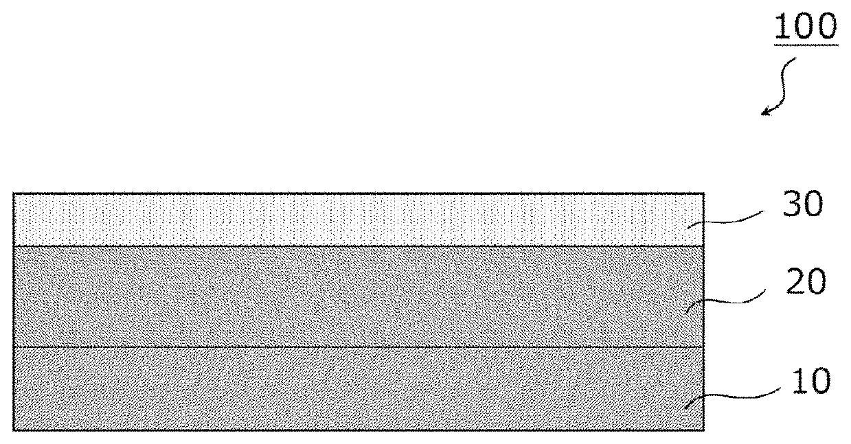
Provided is a pressure-sensitive adhesive tape for protecting a semiconductor that can satisfactorily fill an uneven surface and is prevented from an adhesive residue. The pressure-sensitive adhesive tape for protecting a semiconductor includes: a base material; a pressure-sensitive adhesive layer arranged on at least one side of the base material; and an intermediate layer arranged between the base material and the pressure-sensitive adhesive layer, wherein a storage modulus of elasticity A (MPa) of the pressure-sensitive adhesive layer, a thickness B (μm) of the intermediate layer, a thickness C (μm) of the pressure-sensitive adhesive layer, and a tack value D (N) of the pressure-sensitive adhesive layer satisfy the formula A×(B / C)×D≥20 (MPa·N).

Description

BACKGROUND OF THE INVENTIONField of the Invention[0001]The present invention relates to a pressure-sensitive adhesive tape for protecting a semiconductor.Description of the Related Art[0002]At the time of the production of a semiconductor chip, a backgrinding step of grinding the back surface of a semiconductor wafer to a desired thickness has heretofore been performed. In the backgrinding step, a pressure-sensitive adhesive tape for protection (backgrinding tape) has been used for fixing the semiconductor wafer or protecting a surface opposite to its surface to be ground (e.g., Japanese Patent Application Laid-open No. 2011-151163). The backgrinding tape typically includes a base material and a pressure-sensitive adhesive layer. Such backgrinding tape is used by bonding its pressure-sensitive adhesive layer side to the front surface of the semiconductor wafer (surface opposite to the surface to be ground of the wafer), and is peeled after the back surface of the semiconductor wafer...

Claims


Application Information

Patent Timeline
Patent Type & Authority Patents(United States)
IPC IPC(8): C09J7/38C09J201/02
CPCC09J7/385C09J201/02C09J2203/326C09J2301/122C09J2301/302Y10T428/28Y10T428/2809Y10T428/2848Y10T428/2891C09J7/22C09J7/50C09J133/066H01L21/6836C09J2433/003C09J7/29C09J2301/312H01L2221/68327H01L2221/68381
Inventor SASAKI, TAKATOSHIMIZUNO, KOUJITODA, TAKAYUKI
Owner NITTO DENKO CORP
Why Eureka
Try Eureka