Supercharge Your Innovation With Domain-Expert AI Agents!

SSD architecture supporting low latency operation

a low-latency, ssd technology, applied in the direction of input/output to record carriers, instruments, computing, etc., can solve the problems of collision between i/o, i/o latency, and the amount of time it takes to complete an i/o operation

Active Publication Date: 2022-04-05
TOSHIBA MEMORY CORP
View PDF9 Cites 4 Cited by
  • Summary
  • Abstract
  • Description
  • Claims
  • Application Information

AI Technical Summary

Benefits of technology

The patent describes a solid state drive (SSD) that can assign physical blocks of non-volatile memory dies to different regions for read and write operations. The SSD can also create namespaces and maintain a maintenance counter for each region to manage data operations. The technical effect of this design is improved performance and efficiency of the SSD, allowing for faster read and write operations and reduced maintenance costs.

Problems solved by technology

While such an SSD architecture maximizes the bandwidth or throughput of an SSD, this architecture also suffers from a number of issues that impact I / O latency (i.e., the amount of time it takes to complete an I / O operation).
Due to physical limitations of the non-volatile memory dies, only a single physical block per plane per non-volatile memory die can perform an I / O operation at a time, which leads to collisions between I / O operations to different physical blocks of the same plane of the same non-volatile memory die where an I / O operation must wait until the previous operation to a different block in the same plane has completed.
Relatedly, because there are multiple non-volatile memory dies per channel controller, there may also be collisions between commands for I / O operations to different superblocks at the channel controller, due to the shared nature of a channel in which only one data transfer may proceed at any time between the controller and any non-volatile memory die, leading to bottlenecks at each channel controller of the SSD.
These maintenance operations take place at typically indeterminate times throughout the lifetime of the SSD as needed and last for an indeterminate period of time, which inevitably lead to collisions with host I / O operations at both the channel controllers and the non-volatile memory dies.
These collisions, either due to host I / O operations or SSD maintenance operations causes inconsistent and unpredictable SSD latency performance.
However, if there is a collision, the latency of the read operation may be greatly increased.
Even worse, if a maintenance operation is currently being performed, such as garbage collection which requires all three of a read, a write, and an erase operation, the latency of the read operation to a physical block of a non-volatile memory die currently undergoing maintenance may be significantly greater—in the millisecond range to complete the read operation.
This problem is further exacerbated in a data center or storage center environment storing data across large numbers of SSDs that are being constantly accessed by multiple host applications (i.e., the SSDs are constantly being written to and read from), greatly increasing the likelihood of collisions between I / O operations and maintenance operations.
Given the ever increasing need for storage in data centers and the growing popularity of cloud-based and web-based applications, the inconsistent and unpredictable SSD performance provided by conventional SSD architectures focused on achieving high average bandwidth is no longer sufficient to meet the current demands and requirements of such consumers.

Method used


Image

  • SSD architecture supporting low latency operation
  • SSD architecture supporting low latency operation
  • SSD architecture supporting low latency operation

Examples


Embodiment Construction

[0026]Part 1: I / O Determinism and the SSD Architecture Supporting I / O

Determinism for Low Latency Operation

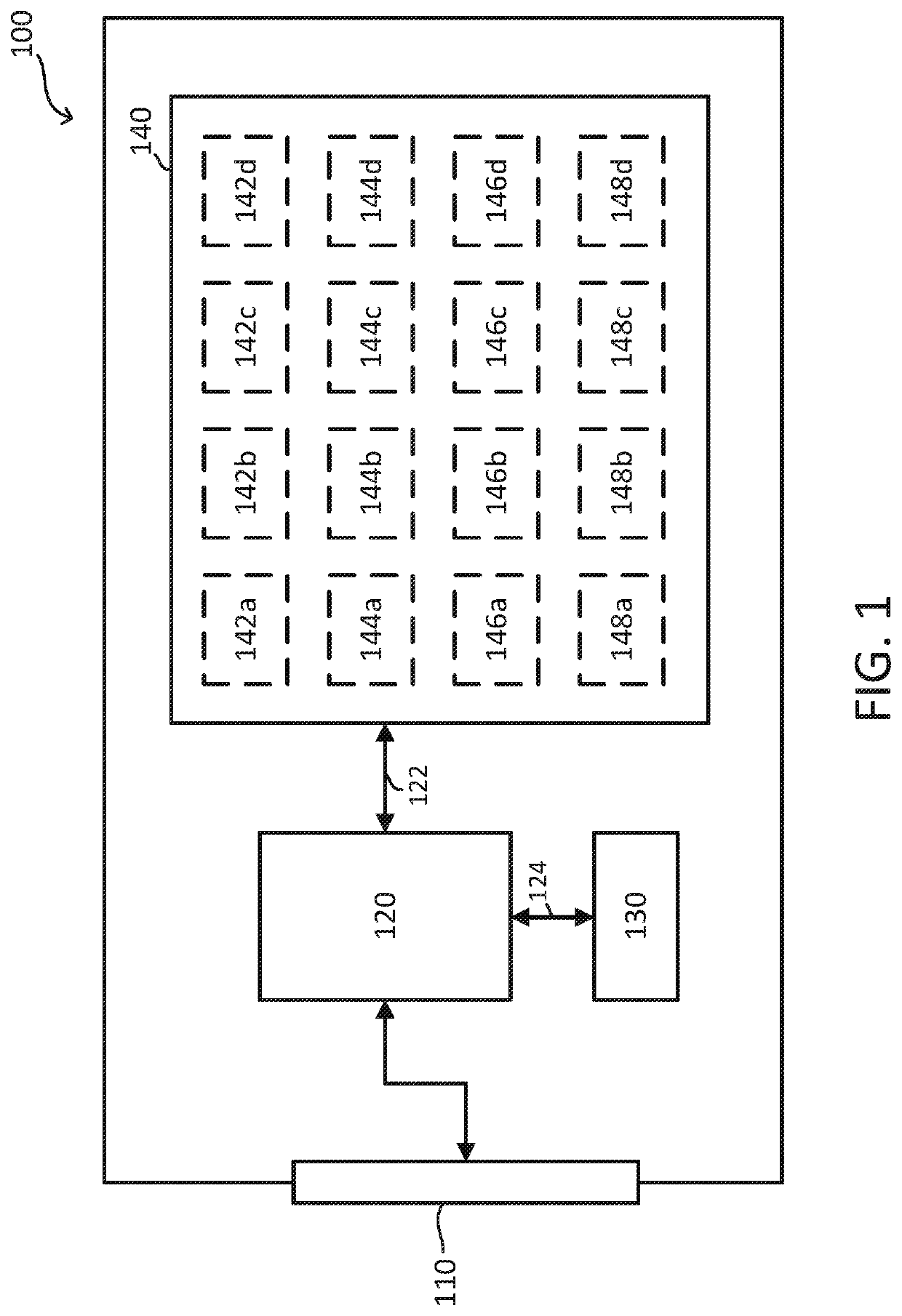
[0027]FIG. 1 is a block diagram of the structure of an SSD 100, according to one embodiment of the invention. As shown in FIG. 1, an SSD memory controller 120 is in communication with one or more host devices or host applications (not shown) through a host interface 110. The host device may comprise any suitable device, such as a computer or storage appliance. The SSD 100 includes both a volatile memory 130, and an array of non-volatile memory dies 140. The volatile memory device 130 and the array of non-volatile memory dies 140 are in communication 124 and 122, respectively, with the SSD memory controller 120.

[0028]The array of non-volatile memory dies 140 comprises non-volatile memory dies 142a-d, 144a-d, 146a-d, and 148a-d that may be arranged in one or more channels in communication 122 with the SSD memory controller 120. While 16 non-volatile memory dies 142a-d, 144a-d, 146...


PUM


Abstract

In one embodiment, a solid state drive (SSD) comprises a plurality of non-volatile memory dies communicatively arranged in one or more communication channels, each of the plurality of non-volatile memory dies comprising a plurality of physical blocks, one or more channel controllers communicatively coupled to the one or more communication channels, respectively, and a memory controller communicatively coupled to the plurality of non-volatile memory dies via the one or more channel controllers, wherein the memory controller is configured to assign (i) the plurality of physical blocks of a first die of the plurality of non-volatile memory dies to only a first region and (ii) the plurality of physical blocks of a second die of the plurality of non-volatile memory dies to only a second region, perform only read operations on the first region in a first operation mode, and perform write operations or maintenance operations on the second region in a second operation mode concurrently with read operations on the first region in the first operation mode.

Description

RELATED APPLICATION[0001]This application claims the benefit of provisional application No. 62 / 542,108 filed on Aug. 7, 2017, which is incorporated herein by reference in its entirety.FIELD OF THE INVENTION[0002]This invention generally relates to solid state drive (SSD) architectures, and more particularly, to SSD architectures supporting low latency operation.BACKGROUND OF THE INVENTION[0003]Conventionally, SSD architectures and designs have primarily focused on obtaining a high average bandwidth or throughput for input and output (I / O) operations (i.e., reading and writing data). Compared to traditional magnetic storage devices such as hard disk drives (HDDs), SSDs are capable of performing I / O operations that are hundreds, if not thousands, of times greater per second as compared to HDDs. Such conventional SSDs are capable of obtaining such high average bandwidth through parallelism in its architecture.[0004]An SSD typically comprises a number of non-volatile memory dies, such a...

Claims


Application Information

Patent Timeline
Patent Type & Authority Patents(United States)
IPC IPC(8): G06F3/06
CPCG06F3/0659G06F3/061G06F3/0611G06F3/0644G06F3/0679G06F3/0613G06F3/0638G06F3/0688G06F11/1008G06F11/1048
Inventor WELLS, STEVENCARLSON, MARKJAIN, AMITKOTTE, NARASIMHULU DHARANITHANGARAJ, SENTHILMISHRA, BARADADESAI, GIRISH
Owner TOSHIBA MEMORY CORP
Features
  • R&D
  • Intellectual Property
  • Life Sciences
  • Materials
  • Tech Scout
  • Unparalleled Data Quality
  • Higher Quality Content
  • 60% Fewer Hallucinations
Learn More