Layout structure between substrate, micro-LED array and micro-vacuum module for micro-LED array transfer using micro-vacuum module, and method for manufacturing micro-LED display using the same

Active Publication Date: 2022-04-05
KOREA ADVANCED INST OF SCI & TECH
View PDF11 Cites 0 Cited by
  • Summary
  • Abstract
  • Description
  • Claims
  • Application Information

AI Technical Summary

Benefits of technology

[0022]A method for transfer and assembly of a RGB micro-light-emitting diode using vacuum suction force according to the present disclosure provides physical bonding and electrical connection between a micro-light-emitting diode and a target substrate at the same time through a process of aligning and transferring micro-light-emitting diodes of red, blue and green colors formed on a mother substrate to desired positions on a target substrate coated with a transfer member, and deforming the transfer member by applying an external force onto the transferred micro-light-emitting diodes using any means.
[0023]That is to say, a

Problems solved by technology

For polymer stamping, the type of devices that can be transferred are limited, for example, only to low-efficiency horizontal micro-LEDs.
In addition, as the stamp size is increased, large-area transfer becomes difficult due to drooping of the stamp, which leads to low transfer yield.
The electrostatic transfer module is disadvantageous in that transfer yield is low.
In addition, there is a risk of device failure because a high voltage is applied to the device when the electrostatic force is formed.
The electromagnetic transfer module is also disadvantageous in that transfer yield is low because transfer should be performed at least two times. In addition, it cannot be used for semiconductors with a size of 30 μm or smaller.
However, because the transfer process of mounting very small LED ch

Method used


Image

  • Layout structure between substrate, micro-LED array and micro-vacuum module for micro-LED array transfer using micro-vacuum module, and method for manufacturing micro-LED display using the same
  • Layout structure between substrate, micro-LED array and micro-vacuum module for micro-LED array transfer using micro-vacuum module, and method for manufacturing micro-LED display using the same
  • Layout structure between substrate, micro-LED array and micro-vacuum module for micro-LED array transfer using micro-vacuum module, and method for manufacturing micro-LED display using the same

Examples


Example

BEST MODE

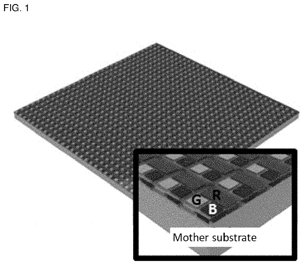
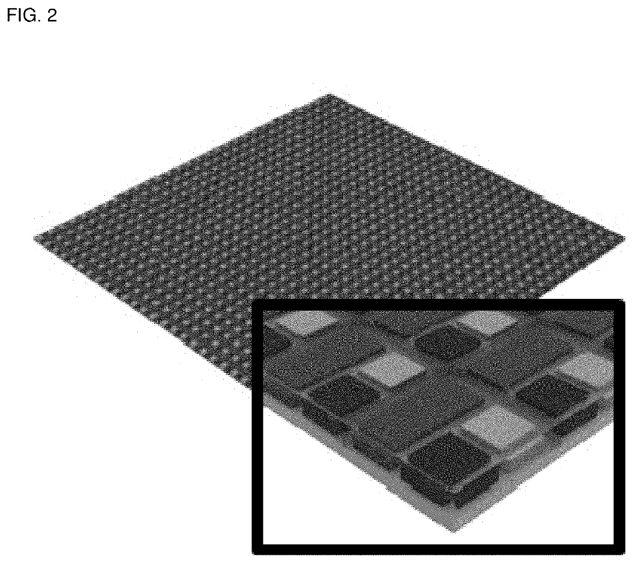
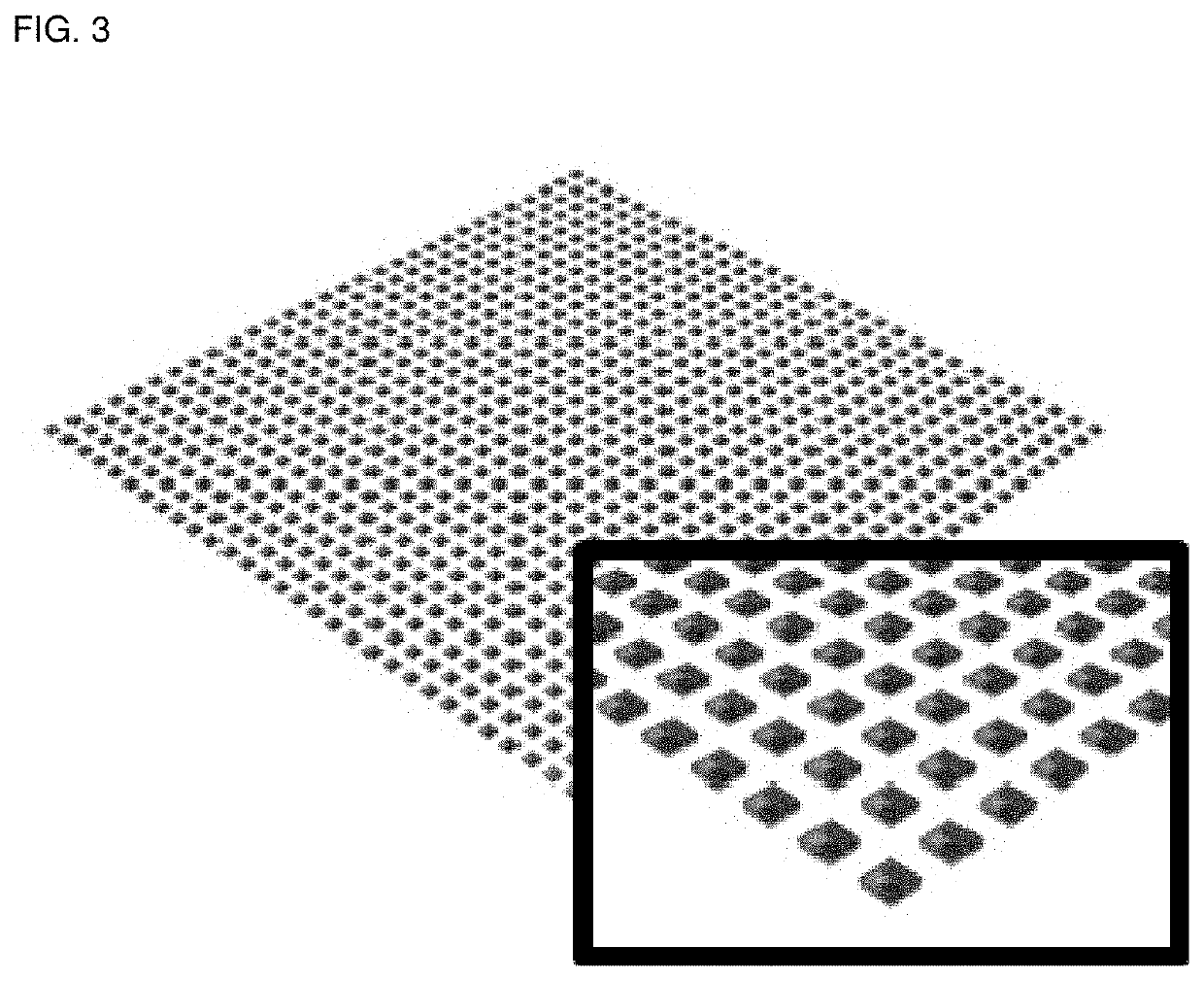
[0041]Hereinafter, the present disclosure will be described in detail through examples. However, the following examples are for illustrative purposes only and it will be apparent to those of ordinary skill in the art that the scope of the present disclosure is not limited by the examples.

[0042]All the factors relating to the processes in the present disclosure, including a mother substrate on which micro-LEDs are formed, a target substrate to which the micro-LEDs are transferred, a transfer member coated on the target substrate, an external force-applying means applying external force to the micro-LEDs transferred onto the target substrate, etc. are applied identically to both chip-type micro-LEDs and thin film-type micro-LEDs.

[0043]A micro-vacuum module performing micro-vacuum adsorption in the present disclosure has a process substrate on which a first connection hole connected to an external pump module and a second connection hole connected to a vacuum controller are fo...


PUM


Abstract

The present disclosure provides a method for transfer and assembly of RGB micro-light-emitting diodes using vacuum suction force whereby the vacuum state of micrometer-sized adsorption holes to which micro-light-emitting diodes formed on a mother substrate or a temporary substrate are bonded is controlled selectively, so that only the micro-light-emitting diode devices desired to be detached from the mother substrate or the temporary substrate are detached from the mother substrate or the temporary substrate using vacuum suction force and then transferred to a target substrate.

Description

CROSS-REFERENCE TO RELATED APPLICATIONS[0001]This application is a Continuation in part of U.S. patent application Ser. No. 16 / 225,178 filed on Dec. 19, 2018, which claims benefit of priority under 35 USC § 119(a) to Korean Patent Application Nos. 10-2018-0067701 filed on Jun. 12, 2018 and 10-2018-0076935 filed on Jul. 3, 2018 in the Korean Intellectual Property Office, the entire disclosures of which are incorporated herein by reference for all purposes.TECHNICAL FIELD[0002]The present disclosure relates to a method for vacuum suction force-based easy transfer and assembly of RGB micro-light-emitting diodes formed on a mother substrate as chips or thin films onto a target substrate by detaching the micro-light-emitting diodes from the mother substrate using selective micro-vacuum adsorption.BACKGROUND ART[0003]The existing printable semiconductors include thin film transistors, micro-LEDs, batteries, memories, etc. In general, the semiconductor is formed on a hard mother substrate ...

Claims


Application Information

Patent Timeline
IPC IPC(8): H01L21/683H01L21/677B65G47/91H01L33/62
CPCH01L21/67721B65G47/91H01L21/6838H01L33/62H01L25/0753H01L33/0095H01L21/6835H01L21/6836H01L2221/68327H01L2221/68368H01L2221/68322
Inventor LEE, KEON JAELEE, HAN EOLKIM, TAE JINSHIN, JUNG HOPARK, SANG HYUN
Owner KOREA ADVANCED INST OF SCI & TECH
Why Eureka
Try Eureka