Semiconductor device manufacturing method and semiconductor device

a semiconductor device and manufacturing method technology, applied in the direction of sustainable manufacturing/processing, final product manufacturing, printed circuit aspects, etc., can solve the problems of increased cost, increased connection terminal size, and increased probability of damage to contacts into which the connection terminal is press-fitted

Active Publication Date: 2022-04-05
FUJI ELECTRIC CO LTD
View PDF12 Cites 0 Cited by
  • Summary
  • Abstract
  • Description
  • Claims
  • Application Information

AI Technical Summary

Benefits of technology

[0051]According to the present embodiment, it is possible to increase a tensile load of connection terminals fitted into contacts and suppress a drop in reliability of a semiconductor device.

Problems solved by technology

However, in this case, there is a higher probability of damage to the contacts into which the connection terminals are press-fitted and an increase in cost due to the increase in size of the connection terminals.

Method used


Image

  • Semiconductor device manufacturing method and semiconductor device
  • Semiconductor device manufacturing method and semiconductor device
  • Semiconductor device manufacturing method and semiconductor device

Examples


Embodiment Construction

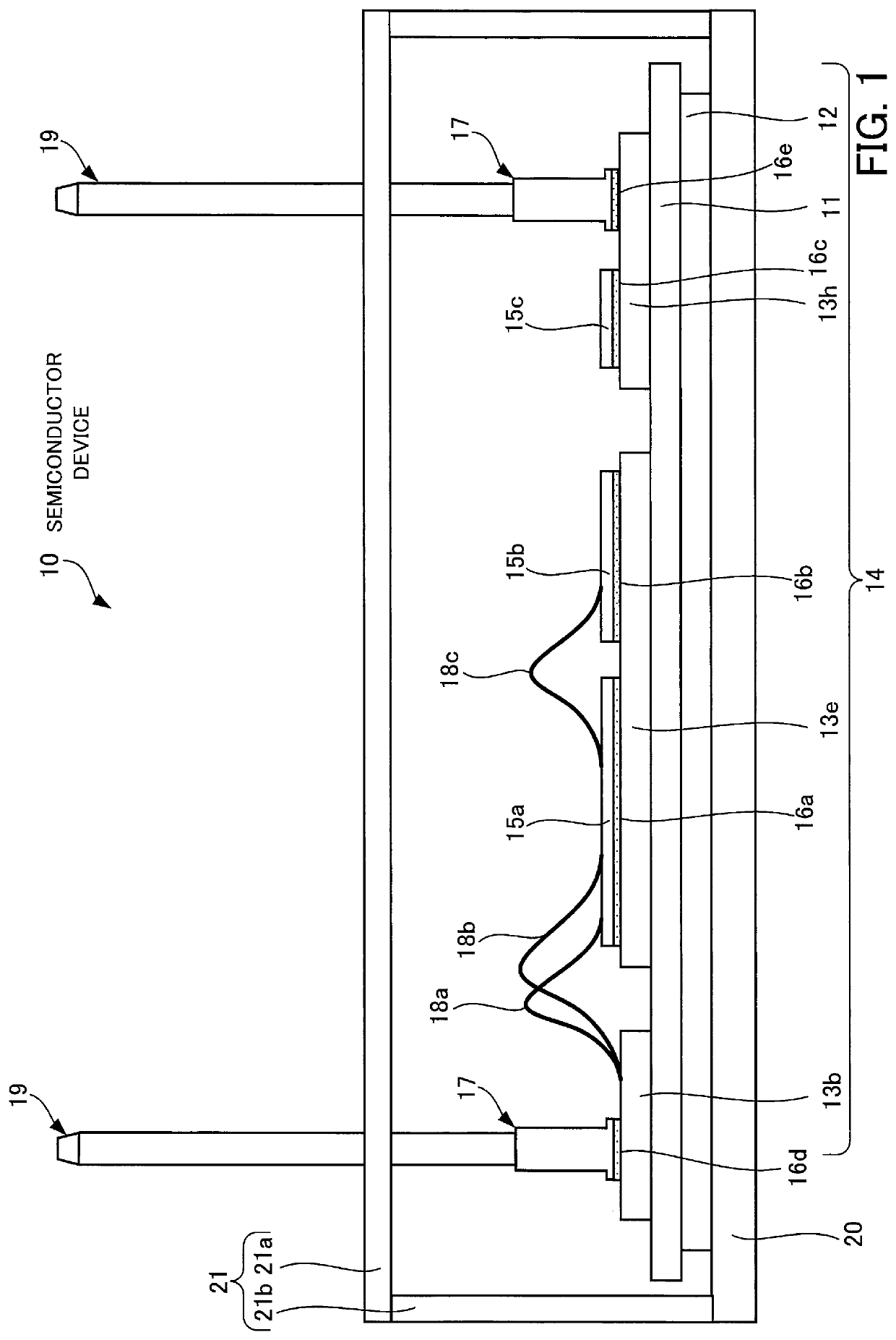
[0021]An embodiment will now be described with reference to the drawings. A semiconductor device according to the present embodiment will now be described with reference to FIG. 1. FIG. 1 depicts one example of a semiconductor device according to the present embodiment. As depicted in FIG. 1, a semiconductor device 10 includes a ceramic circuit board 14, and semiconductor elements 15a, 15b, and 15c and contacts 17 that are provided on a front surface of the ceramic circuit board 14. A column-shaped connection terminal 19 is attached to each of the contacts 17. Note that when no particular distinction is made between them, the semiconductor elements 15a, 15b, and 15c are collectively referred to as the “semiconductor elements 15”. A plurality of semiconductor elements 15 are provided on the ceramic circuit board 14. FIG. 1 depicts the semiconductor elements 15a, 15b, and 15c out of these semiconductor elements 15. Electronic components may be mounted in place of the semiconductor ele...


PUM

PropertyMeasurementUnit
inner diameteraaaaaaaaaa

Abstract

A method of manufacturing a semiconductor device prepares contact members, each of which has a cylindrical through-hole, and column-shaped connection terminals, each having a polygonal shape in a cross-sectional view along a length direction thereof, wherein a length of a diagonal of the polygonal shape is greater than an inner diameter of the through-holes. Chamfers with a curvature for fitting an inner surface of the through-holes are formed at corners of the connection terminal, and the connection terminals are press-fitted into the through-holes of the contacts. By doing so, the area of contact where the connection terminals press-fitted into the contacts contact the inner circumferential surfaces of the through-holes of the contacts is increased. This increases the tensile load of the connection terminals fitted into the contacts.

Description

CROSS-REFERENCE TO RELATED APPLICATION[0001]This application is a continuation application of International Application PCT / JP2019 / 017637 filed on Apr. 25, 2019 which designated the U.S., which claims priority to Japanese Patent Application No. 2018-115687, filed on Jun. 19, 2018, the entire contents of which are incorporated herein by reference.BACKGROUND OF THE INVENTION1. Field of the Invention[0002]The embodiment discussed herein relates to a semiconductor device manufacturing method and a semiconductor device.2. Background of the Related Art[0003]Semiconductor devices include semiconductor elements such as IGBTs (Insulted Gate Bipolar Transistors) and power MOSFETs (Metal Oxide Semiconductor Field Effect Transistors). These semiconductor devices are used for example as power converting devices.[0004]A semiconductor device includes a board with an insulating plate and a plurality of circuit patterns formed on a front surface of the insulating plate. Semiconductor elements and co...

Claims


Application Information

Patent Timeline
Patent Type & Authority Patents(United States)
IPC IPC(8): H01L23/053H01L21/48H01L23/373H01L23/00H01L25/07H01L23/13
CPCH01L23/053H01L21/4817H01L23/3735H01L24/73H01L25/072H01L23/13H01L2224/73265H01L2924/207H01L2224/48137H01L2224/48472H01L2224/48091H01L2224/48227H01L2224/32225H01L25/18H01L23/49811H05K3/4015H01L21/4853H05K2201/10257H05K2201/1031H05K2201/10318Y02P70/50H01L2924/00014H01L2924/00012
Inventor MARUYAMA, RIKIHIROMIYAKOSHI, MASAOKI
Owner FUJI ELECTRIC CO LTD
Why Eureka
Try Eureka