
Semiconductor device

a technology of semiconductor devices and semiconductor modules, applied in semiconductor devices, solid-state devices, power conversion systems, etc., can solve the problems of potential fluctuation deterioration of conduction noise, reduced area of semiconductor elements, and increased cost, etc., to achieve the effect of suppressing conduction nois

Active Publication Date: 2022-04-12
MITSUBISHI ELECTRIC CORP
View PDF4 Cites 0 Cited by
  • Summary
  • Abstract
  • Description
  • Claims
  • Application Information

AI Technical Summary

Benefits of technology

[0004]The object of the present disclosure is to suppress the conduction noise in a semiconductor device.
[0006]The semiconductor device of the present disclosure includes impedance provided between each of the freewheel diodes of an upper arm and the output terminals, and impedance provided between each of the freewheel diodes of a lower arm and the input in the inverter section. Therefore, when the switching of each of the first switching elements is performed at different timing, the current flowing into the inverter section and flowing through the freewheel diodes can be suppressed. Thus, the potential fluctuations of the output terminals are suppressed, and the conduction noise is reduced.

Problems solved by technology

However, under the circumstances where downsizing of semiconductor devices is ongoing, an inevitable reduction in the area of a semiconductor element has been made, and as the improvement in characteristics of semiconductor elements approaches the limit, the thermal design of semiconductor modules has become even harsher.
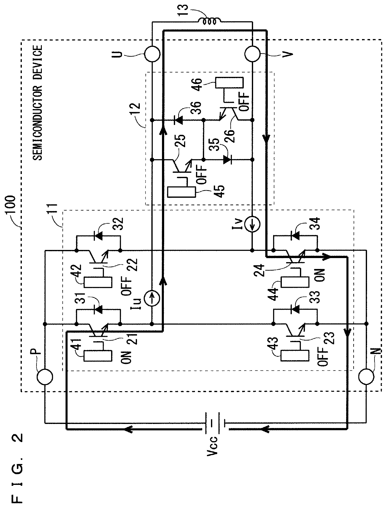
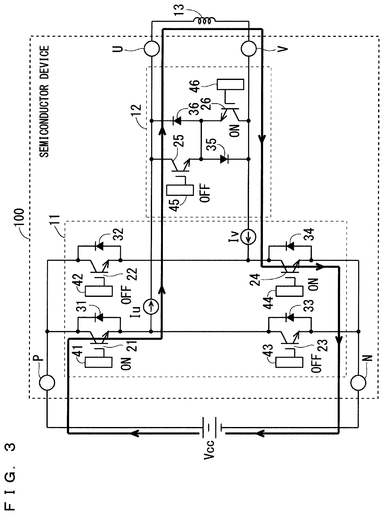
However, the current flowing into the inverter section at the time of reflux causes potential fluctuation at the output terminals in the inverter section, and when high-scale potential fluctuation occurs, the potential fluctuation may possibly deteriorate the conduction noise.

Method used


Image

  • Semiconductor device
  • Semiconductor device
  • Semiconductor device

Examples


embodiment 1

B. Embodiment 1

B-1. Configuration

[0033]FIG. 7 is a circuit diagram of a semiconductor device 101 according to Embodiment 1. The semiconductor device 101 is obtained by adding impedance between the anode of each freewheeling diode 31 to 34 of the inverter section 11 and the output terminals or the input terminal in the HERIC circuit 100 of the underlying technique. Specifically, in the upper arm, impedance 51 is connected between the anode of the freewheel diode 31 of the first-phase IGBT 21 and the output terminal U, and impedance 52 is connected between the anode of the freewheel diode 32 of the second-phase IGBT 22 and the output terminal V. And, in the lower arm, impedance 53 is connected between the anode of the freewheel diode 33 of the third-phase IGBT 23 and the input terminal N and impedance 53, 54 is connected between the anode of the freewheel diode 34 of the fourth-phase IGBT 24 and the input terminal N.

[0034]The impedances 51 to 54 are greater than parasitic impedance of...

embodiment 2

C. Embodiment 2

C-1. Configuration

[0038]FIG. 10 is a circuit diagram of a semiconductor device 102 according to Embodiment 2. The semiconductor device 102 is different from the semiconductor device 101 of Embodiment 1 in that the IGBTs 21 to 24 and the freewheel diodes 31 to 34 have different connection paths toward the output terminals U and V or toward the input terminal N.

[0039]Specifically, in the semiconductor device 102, the IGBT 21 is connected to the output terminal U through a path different from that of the freewheel diode 31 connected in antiparallel to the IGBT 21. Also the IGBT 22 is connected to the output terminal V through a path different from that of the freewheel diode 32 connected in antiparallel to the IGBT 22. Also the IGBT 23 is connected to the input terminal N through a path different from that of the freewheel diode 33 connected in antiparallel to the IGBT 23. Also the IGBT 24 is connected to the input terminal N through a path different from that of the fre...

embodiment 3

D. Embodiment 3

C-1. Configuration

[0048]The circuit diagram of the semiconductor device 103 of Embodiment 3 is as illustrated in FIG. 10, and is similar to the semiconductor device 102 of Embodiment 2.

[0049]FIG. 12 illustrates the internal structure of the semiconductor device 103. In the semiconductor device 103, the anodes of the freewheel diodes 31 to 34 of the inverter section 11 are connected to the electrode pattern 63 corresponding to the output terminals U and V or the input terminal N by the external wiring 69. The external wiring 69 constitutes the impedances 51 to 54. In other respects, the semiconductor device 103 is similar to the semiconductor device 102. The external wiring 69 is also referred to as second external wiring.

D-2. Effect

[0050]In the semiconductor device 103 of Embodiment 3, the anodes of the freewheel diodes 31 and 32 are connected to the output terminals U and V, respectively, in the upper arm and the anodes of the freewheel diodes 33 and 34 are connected...


PUM

PropertyMeasurementUnit
parasitic impedanceaaaaaaaaaa
impedancesaaaaaaaaaa
impedanceaaaaaaaaaa

Abstract

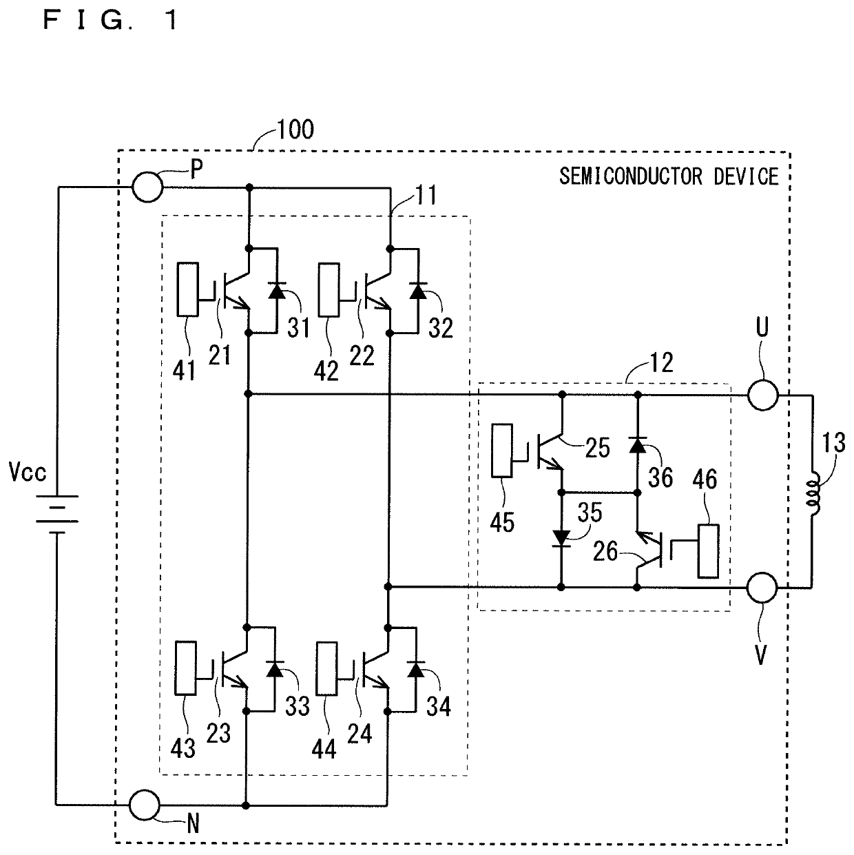
The object of the present disclosure is to suppress the conduction noise in a semiconductor device. A semiconductor device includes an inverter section being a full-bridge inverter, and a reflux section that short-circuits between output terminals U and V of the inverter section, in which impedances and are provided between each of freewheel diodes and of the upper arm and the output terminals U and V, and impedances and are provided between the freewheel diodes and of the lower arm and the input terminal N of in the inverter section, and the impedances to are greater than parasitic impedance of wiring assuming that IGBTs to and the output terminals U and V or the IGBTs and the input terminal N are connected only by the wiring.

Description

BACKGROUND OF THE INVENTIONField of the Invention[0001]The present disclosure relates to a semiconductor device.Description of the Background Art[0002]In the field of semiconductor devices, thinning of semiconductor elements has conventionally been performed in order to suppress a temperature rise generated when a semiconductor operates. However, under the circumstances where downsizing of semiconductor devices is ongoing, an inevitable reduction in the area of a semiconductor element has been made, and as the improvement in characteristics of semiconductor elements approaches the limit, the thermal design of semiconductor modules has become even harsher.[0003]In recent years, in power converters such as inverters, a highly efficient and reliable inverter concept (HERIC) circuit in which a full-bridge inverter and a switching element that is short-circuited are combined has been used for improving heat radiation (see Japanese Patent Application Laid-Open No. 2017-17842). The inverte...

Claims


Application Information

Patent Timeline
Patent Type & Authority Patents(United States)
IPC IPC(8): H02M1/44H02M1/088H02M7/5387H01L25/18
CPCH02M1/44H02M1/088H02M7/5387H01L25/18H02M1/32H02M7/53871H02M7/003H01L2924/13055H01L2924/1203H01L2924/3011H01L2924/19043H01L2924/19105H01L2224/04042H01L2224/49175H01L2224/48227H01L2224/73265H01L25/072H01L2924/13091H01L2924/10272H01L24/48H01L24/49
Inventor EGUCHI, KEISUKE
Owner MITSUBISHI ELECTRIC CORP
Learn More