Method of manufacturing OTS device, and OTS device

a manufacturing method and technology of ots, applied in the direction of semiconductor devices, basic electric elements, electrical apparatus, etc., can solve the problems of difficult to carry out etching treatment at one time, unstable character of ots devices, etc., to achieve low-cost manufacturing process, reduce irregularities, and simplify processing

Active Publication Date: 2022-05-17
ULVAC INC
View PDF20 Cites 0 Cited by
  • Summary
  • Abstract
  • Description
  • Claims
  • Application Information

AI Technical Summary

Benefits of technology

[0015]The method of manufacturing an OTS device according to the first aspect of the invention includes the step A to the step F and removes the second conductor, all of the OTS portion, and the upper portion of the first conductor by an etching treatment at one time (once) using Ar gas in the step E in the depth direction of the region which is not coated with the resist. Consequently, on the cross-sectional surface of the layered body configured of the second conductor that was subjected to etching, the OTS portion, and the upper portion of the first conductor, it is possible to process the layered body so as to obtain the shape such that the side surfaces of the second conductor, the OTS portion, and the first conductor are on the same plane.
[0016]Conventionally, chemical reaction etching (chemical reaction etching) has been carried out for each of members constituting a layered body by use of an individual gas. In contrast, according to the method of manufacturing an OTS device according to the first aspect of the invention, since the layered body can be removed by an etching treatment at one time (once), simplified processing is achieved, and a low-cost manufacturing process can be realized.
[0017]It is preferable that, when such layered body is formed, the step A, the step B, and the step C be all carried out in a space under reduced pressure and that such three steps A, B, and C be sequent in-situ process. Because of this, the surface of the first conductor formed on the substrate is flattened by the step A, and irregularities are less likely to be generated thereon. Accordingly, irregularities are also suppressed from being generated on the surfaces of the OTS portion and the second conductor which are formed and layered on the first conductor in order. Thus, in the case where a voltage is applied to the OTS portion by the conductors located above and below the OTS portion, since concentration phenomenon of a field is less likely to occur, stability of a device (OTS device) is achieved.
[0018]Furthermore, the step X is carried out between the step A and the step B, and the step X causes the surface of the first conductor formed by the step A to be subjected to a flattening treatment by an inductively-coupled plasma (ICP: Inductively Coupled Plasma) method using Ar gas. For this reason, the flattening of the aforementioned first conductor is further improved.
[0019]Therefore, in the method of manufacturing an OTS device according to the first aspect of the invention, the layered body configured of the first conductor, the OTS portion, and the second conductor (metal-active-metal layer) is formed by in-situ process, and the layered body can be processed by etching at one time (once). Consequently, the method of manufacturing an OTS device according to the first aspect extremely easily contributes to manufacture of crossbar type memory. For this reason, the invention is effective in the field of resisitive memories such as ReRAM, CBRAM, or the like in which use of OTS is expected in future, and memories having a crossbar structure.
[0020]The OTS device according to the second aspect of the invention includes a first conductor, an OTS portion made of chalcogenide, and a second conductor which are layered in order and disposed on an insulating substrate, wherein when surface roughness of the first conductor is defined as Rp-v and a thickness of the OTS portion is defined as Tx, relational expression of Rp-v≤(Tx / 10) is satisfied. Consequently, in the case where a voltage is applied to the OTS portion by the conductors located above and below the OTS portion, stability of a device (OTS device) is achieved.

Problems solved by technology

However, there is a problem in that the aforementioned chalcogenide material used for threshold type selector (Threshold type selector) becomes degraded in threshold voltage (Threshold voltage) due to air exposure and therefore characteristics of the OTS device become unstable.
That is, as a method of forming a layered body including the portion made of chalcogenide and the electrode portions formed at the position above and below thereof, it has been difficult to carry out an etching treatment at one time (once) in a depth direction of the layered body, that is, carry out etching using the same gas without using various gases.

Method used


Image

  • Method of manufacturing OTS device, and OTS device
  • Method of manufacturing OTS device, and OTS device
  • Method of manufacturing OTS device, and OTS device

Examples


experimental example 1

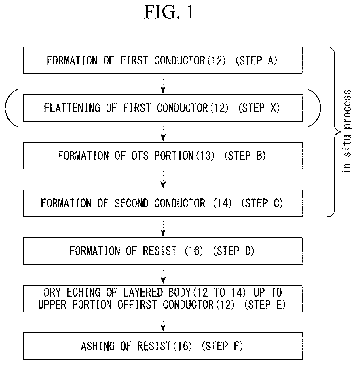
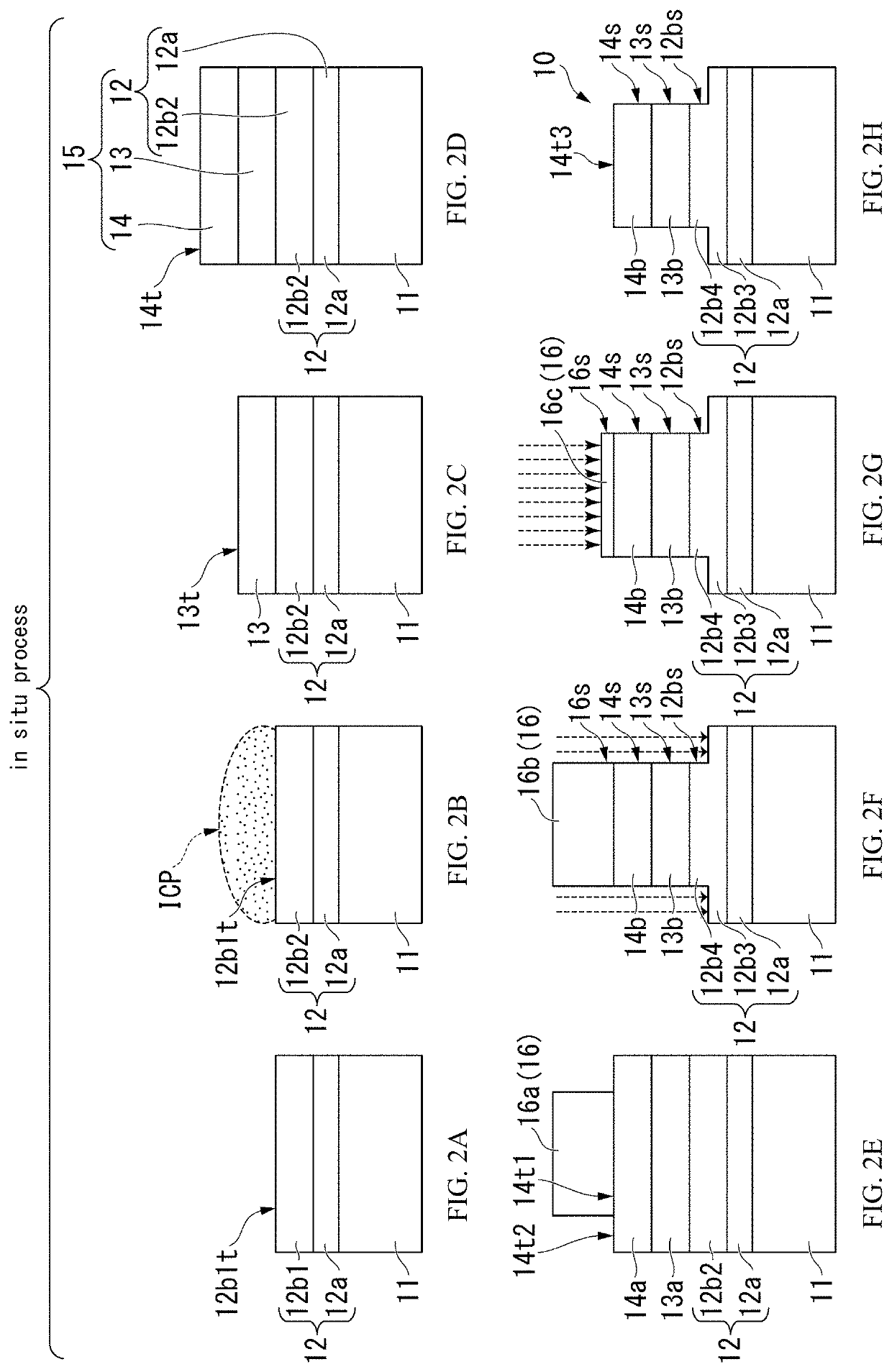
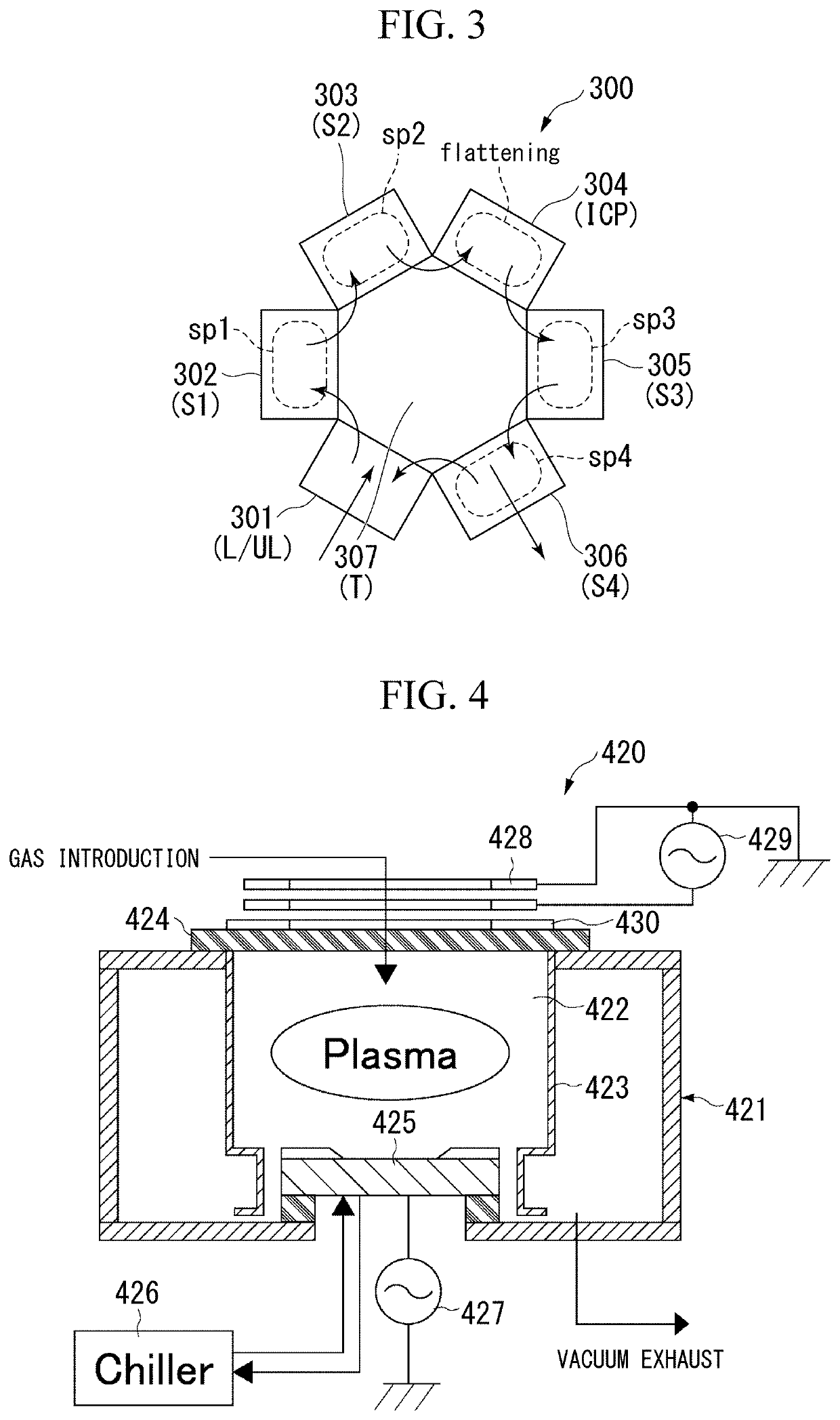
[0085]In the Example 1, in order to evaluate the effects in the case where the series of the processes which are the aforementioned steps A, B, and C were all carried out under a reduced-pressure atmosphere (in-situ process) and the constituent members (first conductor / OTS portion / second conductor) which form the layered body were formed, a first conductor formed of a lower layer (Ti film) / an upper layer (Pt film) was formed by a sputtering method on a substrate formed of Si in the step A. Thereafter, a surface profile of the constituent member formed by the in-situ process was evaluated by use of STM (or AFM).

experimental example 2

[0086]The experimental example 2 is only different from the experimental example 1 in that an ICP process (step X) is carried out on a surface of the first conductor in in-situ process after the first conductor was formed by the sputtering method in the step A and before carrying out the step B. The other points were the same as those of the experimental example 1.

experimental example 3

[0087]The experimental example 3 is only different from the experimental example 1 in that the first conductor is exposed to an air atmosphere after the first conductor was formed by the sputtering method in the step A and before carrying out the step B. The other points were the same as those of the experimental example 1.

[0088]Table 1 is a list including film formation conditions common to the experimental examples 1 to 3. As a processing gas, Ar gas was only used except for the TiN film. In the case of the TiN film, a mixed gas including Ar and N2 was used. Only for the Ti film, film formation was carried out at a room temperature. For the other films, film formation was carried out at 150° C.

[0089]Note that, Table 1 also shows film formation conditions of a Mo film that can be used instead of the TiN film constituting the second conductor.

[0090]In Table 1, Working Pressure represents a pressure during formation, Power represents electric power applied to a target, Ar Flow repres...


PUM

PropertyMeasurementUnit
surface roughness Rpaaaaaaaaaa
surface roughness Rp-aaaaaaaaaa
applied voltageaaaaaaaaaa

Abstract

A method of manufacturing an OTS device of the invention is a method of manufacturing OTS device including a first conductor, an OTS portion made of chalcogenide, and a second conductor which are layered in order and disposed on an insulating substrate. The manufacturing method includes: a step D of forming a resist so as to coat part of an upper surface of the second conductor; a step E of dry etching a region which is not coated with the resist; and a step F of ashing the resist. In the step E, the second conductor, all of the OTS portion, and an upper portion of the first conductor are removed by an etching treatment once in a depth direction of the region.

Description

TECHNICAL FIELD[0001]The present invention relates to a method of manufacturing an OTS device that can achieve stable characteristics of an ovonic threshold switch (OTS: Ovonic Threshold Switch) device.BACKGROUND ART[0002]As the evolution of electronic devices based on Si has reached its limits, innovative operating mechanisms and innovative materials are expected. Among these, chalcogenide (chalcogenide (for example, Ge—Se, Ge—Se—Si, or the like)) glass has excellent electric characteristics and thereby has been attracted attention as the aforementioned material (Non-Patent Document 1). The excellent electric characteristics are the characteristics referred to as threshold switch (TS: Threshold Switch) operation. Accordingly, a phase change memory (phase-change-memory) is commercialized which is a diode selector known as a non-volatile memory device and utilizes a phenomenon referred to as TS crystallization.[0003]Furthermore, such OTS is a hopeful candidate for other devices, for ...

Claims


Application Information

Patent Timeline
Patent Type & Authority Patents(United States)
IPC IPC(8): H01L45/00
CPCH01L45/1675H01L45/1253H01L45/06H01L45/1233H01L45/148H01L21/027H01L21/3065H01L21/321H01L21/3213H01L27/105H10N70/20H10N70/826H10N70/841H10N70/882H10N70/063H10B99/00H01L21/32115H01L21/32136H10N70/011H10N70/231H10N70/884
Inventor AHN, HYUNG-WOOHORITA, KAZUMASASAWADA, TAKAHIKOYAMAMOTO, TADASHI
Owner ULVAC INC
Why Eureka
Try Eureka