Check patentability & draft patents in minutes with Patsnap Eureka AI!

Pixel driving method

a driving method and pixel technology, applied in the field of display technology, can solve the problems of increasing the driver ic load, increasing the cost, and being unable to operate properly, and achieve the effect of increasing the cos

Active Publication Date: 2022-05-24
TCL CHINA STAR OPTOELECTRONICS TECH CO LTD
View PDF2 Cites 0 Cited by
  • Summary
  • Abstract
  • Description
  • Claims
  • Application Information

AI Technical Summary

Benefits of technology

This method effectively reduces source driver temperature without increasing costs by adjusting sub-pixel brightness, thus preventing irreversible damage while maintaining cost efficiency.

Problems solved by technology

A faster scan speed will inevitably lead to an increase in the driver IC loading, especially under the overload display screen (such as all red and blue sub-pixels have a gray scale of 0, all green sub-pixels have a gray scale of 255).
The source driver that is too hot can be dangerous, causing irreversible damage to the source driver, making it impossible to operate properly.
However, the increase in heat sinks undoubtedly lead to an increase in cost.

Method used


Image

  • Pixel driving method
  • Pixel driving method
  • Pixel driving method

Examples


Embodiment Construction

[0047]Structure and technical means adopted by the present disclosure to achieve the above and other objects can be best understood by referring to the following detailed description of the preferred embodiments and the accompanying drawings. Furthermore, directional terms described by the present disclosure, such as upper, lower, front, back, left, right, inner, outer, side, longitudinal / vertical, transverse / horizontal, etc., are only directions by referring to the accompanying drawings, and thus the used directional terms are used to describe and understand the present disclosure, but the present disclosure is not limited thereto.

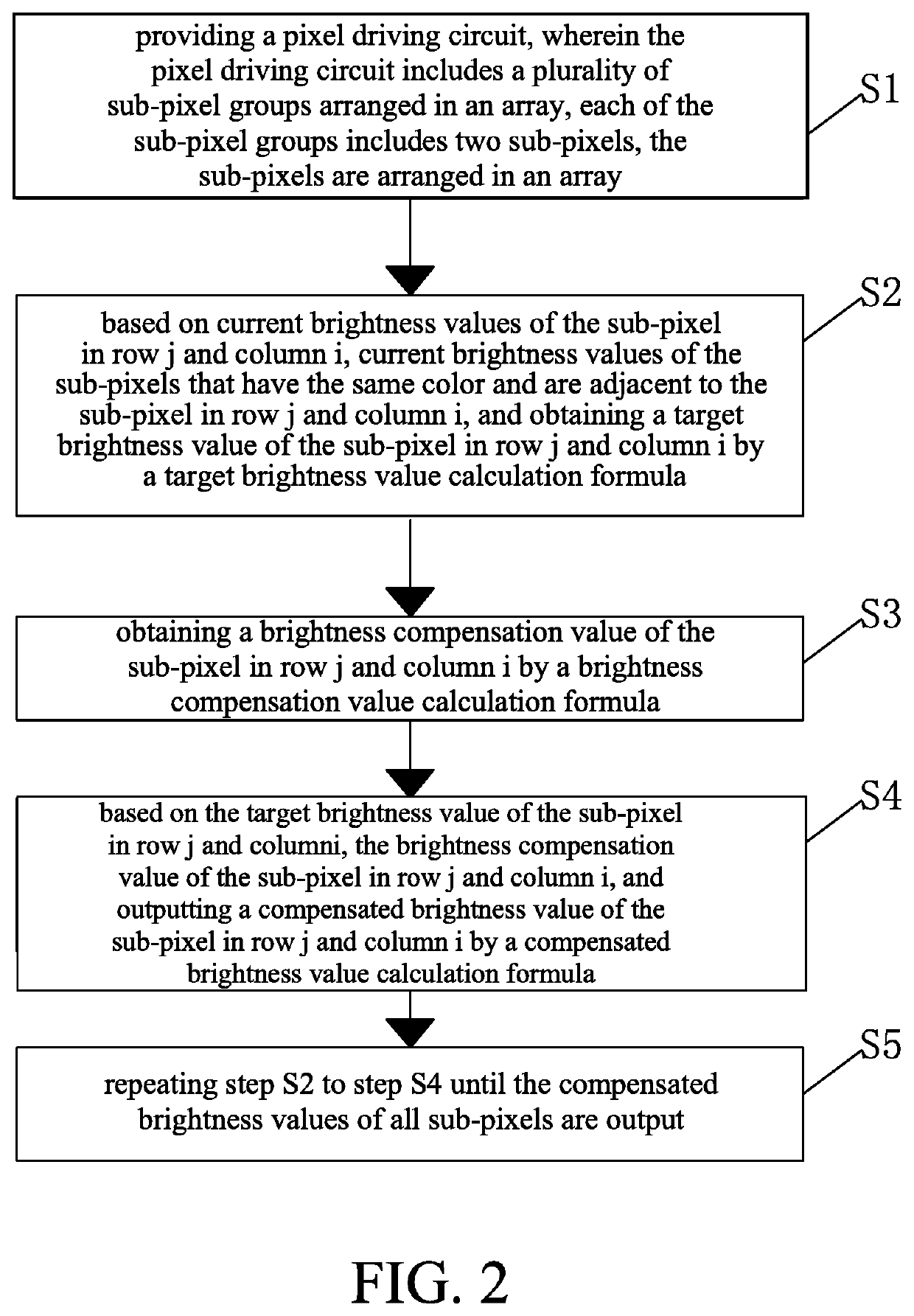
[0048]Referring to FIG. 2, a flowchart of a pixel driving method according to the present disclosure is illustrated. The pixel driving method includes steps of step S1, step S2, and step S3.

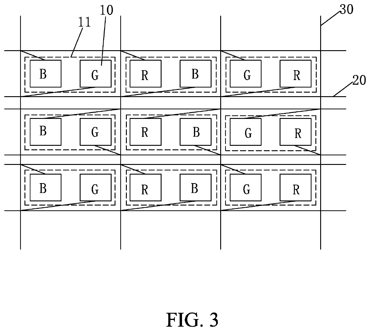
[0049]Referring to FIG. 3, in step S1, a pixel driving circuit is provided, wherein the pixel driving circuit includes a plurality of sub-pixel groups 11 arranged in a...


PUM


Abstract

A pixel driving method is provided. Based on current brightness values of the sub-pixel in row j and column i, current brightness values of the sub-pixels that have the same color and are adjacent to the sub-pixel in row j and column i to obtain the target brightness value of the sub-pixel in row j and column i by the target brightness value calculation formula, and then to obtain a brightness compensation value of the sub-pixel in row j and column i by a brightness compensation value calculation formula, and based on the target brightness value of the sub-pixel in row j and column i, the brightness compensation value of the sub-pixel in row j and column i to output a compensated brightness value of the sub-pixel in row j and column i by a compensated brightness value calculation formula.

Description

FIELD OF INVENTION[0001]The present disclosure relates to a display technology field, and in particular, relates to a pixel driving method.BACKGROUND OF INVENTION[0002]Thin film transistors (TFTs) are main driving components of liquid crystal displays (LCDs) and active matrix organic light-emitting diodes (AMOLEDs). They are directly related to display performance of a flat panel display device.[0003]Most of the liquid crystal displays in the current market are backlight type liquid crystal displays, which include a liquid crystal display panel and a backlight module. The working principle of the liquid crystal display panel is to fill liquid crystal molecules between a thin film transistor array substrate (TFT array substrate) and a color filter (CF) substrate, and a pixel voltage and a common voltage are applied on the two substrates, respectively. Rotation direction of the liquid crystal molecules is controlled by an electric field formed between the pixel voltage and the common ...

Claims


Application Information

Patent Timeline
Patent Type & Authority Patents(United States)
IPC IPC(8): G09G3/36
CPCG09G3/3607G09G3/3677G09G3/3688G09G2300/0452G09G2360/16G09G3/3413G09G3/3611G09G2300/0426
Inventor WANG, GENG
Owner TCL CHINA STAR OPTOELECTRONICS TECH CO LTD
Features
  • R&D
  • Intellectual Property
  • Life Sciences
  • Materials
  • Tech Scout
  • Unparalleled Data Quality
  • Higher Quality Content
  • 60% Fewer Hallucinations
Learn More